DFM-ready bare board manufacturing
PCB Fabrication for Boards That Must Build Cleanly
YourPCB supports PCB fabrication for OEM teams that need more than a cheap bare board: DFM review, stackup and finish control, electrical test planning, and a clean handoff into assembly when the board will become a PCBA.

Fabrication Scope and Positioning
PCB fabrication on this page means bare-board manufacturing from a controlled release package: laminate selection, copper imaging, drilling, plating, solder mask, silkscreen, surface finish, profiling, inspection, and electrical test. The page fills a specific site gap. Existing YourPCB pages already cover custom PCB assembly, prototype PCB assembly, and turnkey electronics manufacturing. This service is for the earlier bare-board decision that decides whether assembly starts with stable boards or avoidable questions.
The strongest fit is a prototype, pilot, or low-volume board that needs documented fabrication choices before it enters SMT, through-hole soldering, inspection, or system integration. Commodity 2-layer boards can move quickly, but product boards with impedance notes, heavy copper, tight connectors, odd outlines, or repeat-order expectations need a cleaner release path. That is the difference between buying boards and controlling a manufacturing input.
Standards and Buyer Evidence
Bare PCB quality needs named standards and measurable release evidence. For reference, IPC electronics standards define much of the language used across PCB design, fabrication, and assembly. Printed circuit board manufacturing includes the physical steps that turn CAD data into a tested board, while ISO 9000 quality management explains the system-level logic behind controlled records and repeatable process evidence.
In practical RFQ language, buyers should name the acceptance class, material family, finished thickness, copper weight, surface finish, electrical test requirement, and any IPC-2221 or IPC-6012 design assumptions that affect manufacturability. YourPCB uses those inputs to decide whether the job belongs on a standard FR-4 route or a focused path such as HDI, heavy copper, aluminum, gold finger, castellated module, or backplane fabrication.
PCB Fabrication Capabilities
DFM Before Tooling
CAM review checks drill registration, annular ring, solder mask clearance, copper balance, rout geometry.
Rigid FR-4 Builds
Standard rigid-board work covers simple 1-2 layer prototypes, 4-layer control boards, and multilayer releases that need clear stackup and finish control.
Special Construction Routing
Heavy copper, HDI, aluminum, gold finger, castellated, and backplane boards are routed to focused service paths when the build needs a narrower process window.
Assembly-Ready Planning
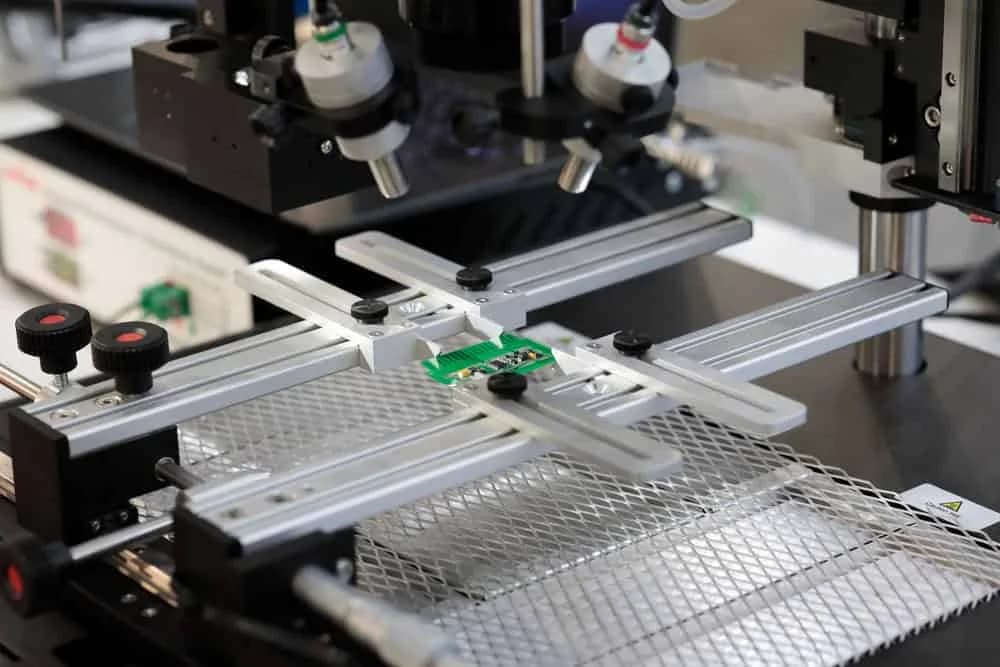
Fabrication choices are reviewed against SMT, through-hole, stencil, panel.
Electrical Test Release
Continuity and isolation testing are planned before shipment so urgent bare boards do not become expensive scrap during first-article assembly.
Repeat Build Control
Revision, finish, stackup, quantity, and release notes stay tied to the order history so the next lot does not depend on memory or undocumented CAM edits.
Capability Table
| Best-fit programs | Prototype, NPI, pilot, bridge, and controlled low-volume PCB builds |
|---|---|
| Core board types | Rigid FR-4, multilayer, heavy copper, HDI, aluminum, castellated, gold finger, and backplane paths |
| Common inputs | Gerber or ODB++, NC drill, outline, stackup notes, quantity, finish, copper weight, and drawing notes |
| Assembly handoff | BOM, XY data, assembly drawing, stencil requirements, inspection notes, and test expectations when PCBA follows |
| Quality references | IPC-A-600, IPC-6012, IPC-2221, ISO 9001:2015 logic, IPC-A-610 for assembled-board acceptance context |
| Inspection planning | CAM review, visual inspection, dimensional checks, electrical test, and special review for impedance or edge features |
| Out of scope | Unreviewed domestic-origin claims, regulatory product certification, or guaranteed impedance without complete stackup data |
First-Hand Scenario: The Finish Choice That Stopped Assembly
A representative pilot build for an industrial sensor used 180 rigid boards, 4 layers, fine-pitch ICs, and a board-to-wire connector near the panel edge. The buyer sent complete Gerbers but left the surface finish as "standard" in the notes. A low-cost fabrication quote assumed HASL. That looked acceptable until the assembly review found a flatness risk for the fine-pitch package and a rework risk around the connector pads.
We paused the release before tooling, changed the quote basis to ENIG, confirmed panel rails for assembly support, and added an electrical test requirement to the fabrication notes. The change added cost at the bare-board stage, but it avoided a more expensive first-article failure after solder paste printing. This is why YourPCB treats fabrication as an assembly input when the board will become a PCBA within the same program.
"A bare board is not finished when it leaves fabrication if the next operation cannot build it cleanly. I want finish, panel, and inspection choices settled before the first stencil is cut."Hommer Zhao, YourPCB technical review
Which PCB Fabrication Path Fits?
The right path depends on the dominant risk. A simple urgent board needs queue control. A power board needs copper and spacing review. A dense BGA board may need HDI planning. A complete product build needs fabrication and assembly decisions under one release plan.
| Buyer situation | Best-fit path | Why it matters |
|---|---|---|
| Simple 2-layer debug board | Prototype PCB fabrication | The buyer needs speed and basic electrical test more than custom stackup control. |
| 4-layer product board for a pilot build | PCB fabrication with assembly handoff | Stackup, finish, fiducials, panelization, and test planning affect both bare-board yield and SMT setup. |
| 4 oz copper power board | Heavy copper PCB fabrication | Etching, spacing, plating, and soldering behavior need a process window that a default FR-4 quote may not cover. |
| Dense BGA board with microvias | HDI PCB manufacturing | Microvia structure, sequential lamination, and registration risk dominate the quote more than ordinary layer count. |
| Bare board plus components, test, labels, and shipment | Turnkey electronics manufacturing | One program owner should manage sourcing, PCB fabrication, assembly, inspection, and final release. |
Fabrication Workflow
1
Quote Package Intake
We check whether the release package contains the fabrication data, drill files, stackup notes, finish, quantity.
2
DFM and Construction Review
Engineering reviews annular ring, spacing, copper balance, slots, edge features, impedance notes, and any mismatch between drawing notes and generated files.
3
Material, Finish, and Panel Plan
The board is aligned with FR-4, high-Tg, heavy copper, aluminum, or other relevant construction paths, then panel and finish choices are locked before tooling.
4
Fabrication and In-Process Checks
Imaging, drilling, plating, solder mask, silkscreen, finish, routing, inspection, and electrical test are controlled against the approved board release.
5
Assembly or Shipment Handoff
Finished boards are released for shipment or paired with stencil, BOM, placement, and inspection planning when the order continues into PCB assembly.

Scope, Limits, and Applications
This service covers fabrication planning and bare-board supply for released PCB designs, including DFM review, construction routing, inspection planning, and assembly handoff when needed. It does not replace electrical design engineering, regulatory product approval, or domestic-origin certification. If a board needs guaranteedcontrolled impedance PCB manufacturing, the quote package must include stackup data, target impedance, trace geometry, layer reference, and material assumptions before the factory can price the requirement properly.
Industrial Controllers
Control boards, I/O modules, power interfaces, and field-service electronics that need repeatable fabrication notes and electrical test records.
Medical and Lab Devices
Pilot builds where board revision, lot traceability, inspection evidence, and later PCBA documentation matter more than a one-time prototype receipt.
Power Electronics
Converters, motor controls, battery equipment, and charging products where copper weight, thermal paths, spacing, and finish affect reliability.
Embedded Hardware
IoT, sensing, instrumentation, and compact devices that need multilayer routing, clean assembly handoff, and stable repeat orders.
Frequently Asked Questions
What files do I need for a PCB fabrication quote?
A PCB fabrication quote should include Gerber or ODB++ files, NC drill data, board outline, layer count, finished thickness, copper weight, solder mask color, silkscreen notes, surface finish, quantity, and delivery target. For 4-layer and higher boards, include stackup intent and impedance notes if traces are controlled. If the boards will move directly into SMT or through-hole assembly, send the BOM, XY placement file, assembly drawing, and test notes in the same package so fabrication choices do not create assembly problems later.
How is PCB fabrication different from PCB assembly?
PCB fabrication makes the bare printed circuit board: laminate, copper layers, drilled holes, plating, solder mask, silkscreen, finish, routing, and electrical test. PCB assembly places and solders components onto that board. The two steps are linked because fabrication choices affect assembly yield. ENIG may help fine-pitch SMT flatness, heavy copper can change thermal balance during soldering, and poor panelization can slow pick-and-place setup. YourPCB reviews fabrication data with the assembly handoff in mind instead of treating bare boards as a disconnected purchase.
I need 50 boards for an engineering pilot. Should I choose prototype or production PCB fabrication?
A 50-board engineering pilot usually needs prototype speed with production-style documentation. Treat it as a controlled pilot when the design will feed regulatory testing, customer demos, or a bridge build above 100 units. The quote should lock board revision, material, finish, stackup, coupon or test expectations, and acceptance class before tooling starts. If the same board will be reordered, request a repeatable fabrication package rather than a one-time bargain prototype, because the second order should not depend on undocumented CAM assumptions.
What standards should I reference for bare PCB fabrication quality?
Bare PCB fabrication quality is commonly discussed around IPC-A-600 for board acceptability, IPC-6012 for rigid printed board performance, IPC-2221 for generic board design guidance, and ISO 9001:2015 for quality management logic. Buyers do not need to quote every clause in an RFQ, but the drawing should state the required class, material family, finish, and electrical test expectation. For assemblies, IPC-A-610 and IPC-J-STD-001 become more relevant after components are soldered.
Can one PCB fabrication supplier support FR-4, heavy copper, HDI, and metal-core boards?
One supplier can coordinate FR-4, heavy copper, HDI, and metal-core PCB fabrication, but each construction needs a different review path. Standard FR-4 boards may pass through normal DFM quickly, while 4 oz copper changes etching and spacing expectations, HDI adds microvia and lamination risk, and aluminum boards change thermal and isolation checks. YourPCB routes these builds through the relevant service path so the quote reflects process risk instead of hiding every board type behind one generic capability list.
How do I reduce PCB fabrication delays before I release files?
The fastest way to reduce PCB fabrication delays is to remove ambiguity before CAM review. Use one revision package, include the drill file, define finished copper and board thickness, state surface finish, mark controlled-impedance nets, and explain slots, cutouts, bevels, or edge plating. A 10-minute file review can prevent a 24-hour quotation loop when the factory has to ask whether a slot is plated, whether the stackup is mandatory, or whether a finish was chosen for shelf life or fine-pitch assembly.
Related Services
FR-4 PCB Manufacturing
Use this path when ordinary rigid-board work still needs controlled laminate, Tg, stackup, and assembly handoff decisions.
Custom Circuit Board Service
Use this path when the board has non-default stackup, copper, finish, mechanical, or product-specific drawing requirements.
Fast Turn PCB Manufacturing
Use this path when schedule compression is the main problem and the board still needs DFM review and electrical test discipline.
Low Volume PCB Manufacturing
Use this path for small-batch fabrication and assembly programs that need bridge production or controlled repeat lots.
PCB Assembly Prototype
Use this path when the first build needs component sourcing, SMT placement, through-hole work, and first-article feedback.
Get a Quote for DFM-Ready PCB Fabrication
Send the fabrication package before the board is treated as a commodity order. A short DFM and handoff review can catch stackup, finish, panel, and inspection issues before they become assembly delays.

Backed by our Shenzhen SMT factory
4 nitrogen reflow ovens
100% 3D SPI & AOI inspection
Per-board MES traceability
01005 component placement