PCBA Optical Quality Control
AOI Inspection PCB Assembly Service
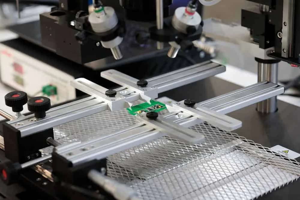
Automated optical inspection only helps when it is tied to the real assembly files, first article findings, defect codes, and downstream test route. YourPCB uses AOI as a release gate for SMT and mixed-technology PCBAs, not as a generic camera pass.
TL;DR
- AOI catches visible SMT placement and solder defects before boards move into expensive downstream steps.
- First article correlation prevents wrong BOM, centroid, or polarity assumptions from becoming production defects.
- AOI does not replace X-ray, ICT, flying probe, or functional testing for hidden or powered failures.
- Useful AOI records connect defects, rework, revision control, and shipment release in one traceable lot file.
What AOI Inspection Actually Proves
Automated optical inspection is a camera-based inspection method that compares an assembled board against programmed rules for component presence, position, polarity, and visible solder condition. Public technical background on automated optical inspection explains the general machine-vision concept, but the buyer result depends on how well the factory connects AOI to the real PCBA release package.
PCB assembly is the process of placing and soldering electronic components onto a circuit board, then verifying workmanship and electrical behavior before shipment. AOI is one inspection gate inside that flow. It can flag visible defects quickly, but it cannot judge hidden solder joints, firmware behavior, or whether a board works in the final product.
YourPCB treats AOI as an engineering control. The inspection route is built around the BOM, centroid file, board finish, polarity evidence, component markings, and known process risks. That is why the strongest AOI programs start before the first production panel reaches the machine.
Capability List
SMT Solder-Joint Review
AOI programs check visible solder fillets, tombstoning, bridging, insufficient solder, component skew, missing parts, and wrong polarity before boards move downstream.
First Article Correlation
The first build is compared against the BOM, centroid data, assembly drawing, polarity marks, silkscreen, and buyer notes before production inspection rules are released.
Defect Code Discipline
Findings are grouped into clear defect codes so engineering can separate real workmanship risk from false calls, documentation mismatch, and cosmetic variation.
Mixed-Technology Handoff
AOI results are aligned with through-hole, selective soldering, X-ray, functional test, and box-build steps so one late defect does not hide inside the system build.
Changeover and Revision Control
Program names, board revisions, panel orientation, BOM alternates, and golden-board references are controlled when a product has variants or repeated small lots.
Buyer-Ready Release Evidence
Lot status, defect trends, rework notes, first article photos, and shipment holds can be tied to the release package when the buyer needs auditable inspection records.
Scope, Limits, and Quote Inputs
| Best-fit builds | SMT PCB assembly, mixed SMT/THT boards, prototype lots, pilot builds, bridge production, and repeat low-volume PCBA programs |
|---|---|
| Typical inputs | Gerbers or ODB++, BOM, pick-and-place data, assembly drawing, polarity notes, panel drawing, revision history, and special acceptance notes |
| Common AOI calls | Missing part, wrong part, offset, skew, tombstone, polarity reversal, lifted lead, solder bridge, insufficient solder, and excess solder |
| Companion inspections | SPI before reflow, X-ray for hidden joints, visual inspection for keep-out or mechanical areas, ICT, flying probe, and functional test |
| Standards context | IPC-A-610 workmanship acceptability, IPC-J-STD-001 soldering process expectations, ISO 9001 record control, and customer-specific drawings |
| Record outputs | First article notes, defect code summary, rework disposition, pass/fail lot status, photos when needed, and shipment release decision |
| Quote variables | Board size, component count, fine-pitch density, double-sided assembly, lot size, required evidence, false-call tolerance, and test sequence |
IPC is an electronics standards organization associated with workmanship documents such as IPC-A-610 and soldering process documents such as IPC-J-STD-001. For public background, see IPC in electronics. ISO 9001 is a quality-management-system standard that supports document control, traceability, and corrective action; its public overview is available at ISO 9000.
AOI is most valuable when the buyer sends the assembly package early. A purchase order that only says inspect boards does not define polarity conventions, acceptable alternates, no-clean flux appearance, cosmetic limits, or what evidence must be saved. The RFQ should include the board data, BOM, placement file, drawing, lot size, and any customer-specific acceptance rules.
Choosing AOI, X-Ray, ICT, or Functional Test
| Buyer situation | Best inspection path | Reason |
|---|---|---|
| Prototype PCBA with new polarity markings | AOI plus first article photo review | The buyer needs early confirmation that the BOM, centroid data, silkscreen, and real component markings agree before repeat builds. |
| Fine-pitch SMT board with QFN or BGA devices | SPI, AOI, and X-ray where joints are hidden | AOI verifies visible placement and solder defects, while X-ray covers hidden solder joints that optics cannot inspect. |
| Mixed SMT and through-hole assembly | AOI before secondary soldering, then visual or selective-solder inspection | The SMT process should be released before connectors, cables, or wave and selective solder steps add more variables. |
| Repeat low-volume build with alternates | AOI rule update tied to BOM revision | Approved alternates can change body color, markings, package height, and polarity cues, so inspection rules need revision control. |
| Box build with PCBA and harness integration | AOI release before enclosure and cable install | Catching board-level workmanship issues before system assembly prevents expensive teardown and unclear root cause after shipment pressure begins. |
X-ray inspection is a radiographic method used when the solder joint or internal feature cannot be seen optically. Functional testing is a powered check that proves the PCBA behaves as the product requires. Those definitions matter because buyers often ask for all inspection without separating visible workmanship, hidden solder risk, and operating behavior.
If your design has BGAs, bottom-terminated packages, high-density connectors, or shield cans, AOI should be paired with the right companion test. Review the AOI buyer guide and first article inspection planning before freezing the release plan.
Release Workflow
1
File and Risk Review
Engineering reviews the BOM, centroid file, Gerbers, assembly drawing, polarity marks, component packages, and known risk areas before the AOI route is set.
2
First Article Setup
The first board or panel is inspected against the released documentation, then questionable calls are corrected before the lot moves through the line.
3
Production AOI
Boards are inspected for placement, solder, polarity, and visible workmanship defects, with suspect assemblies separated for review instead of being pushed downstream.
4
Engineering Disposition
False calls, real defects, rework actions, and documentation corrections are separated so the lot record explains what happened and why.
5
Release and Feedback
Inspection results are tied to shipment release, rework closure, stencil feedback, placement adjustment, or buyer drawing updates for the next build.
Certification and Release Controls
ISO 9001 record control
IPC-A-610 workmanship context
RoHS-aware assembly flow
The practical release package can include first article comments, defect code summaries, rework disposition, test status, and photo evidence when needed. For buyers moving from prototype to repeat lots, the important control is consistency: one board revision, one BOM basis, one inspection route, and one clear shipment decision.
FAQ
What is AOI inspection in PCB assembly?
AOI inspection in PCB assembly is an automated optical inspection step that uses cameras and programmed rules to find visible component placement and solder defects on a PCBA. It is strongest for missing parts, polarity errors, skew, bridges, tombstoning, and visible solder problems. It does not replace X-ray for hidden BGA joints or functional testing for powered behavior.
When should AOI happen in the SMT process?
AOI is usually most useful after reflow because it can confirm whether placement and soldering produced an acceptable assembly. Some programs also use solder paste inspection before reflow, then AOI after reflow, then X-ray or functional test for risks AOI cannot see. The exact sequence depends on board density, package type, and buyer release requirements.
Can AOI inspect every solder joint on a PCBA?
No. AOI can inspect visible joints and component features, but it cannot see under BGA, LGA, bottom-terminated, shielded, or mechanically hidden areas. Those risks need X-ray, electrical test, functional test, or a design change that exposes inspection access. YourPCB treats AOI as one gate in the release plan, not as the only quality proof.
What files do you need to quote AOI inspection with assembly?
Send Gerbers or ODB++, BOM, pick-and-place data, assembly drawing, polarity requirements, panel drawing, board revision, test plan, and any customer-specific acceptance notes. If the product has approved alternates, include the AVL and marking differences so the AOI route does not reject acceptable parts.
How do you reduce false calls during AOI inspection?
False calls are reduced by correlating the first article with the BOM, placement file, real component markings, board finish, lighting, and golden-board references. The goal is not to suppress warnings blindly. The goal is to separate real defects from acceptable variation, then keep the rule set tied to the approved revision.
Can AOI records support a multi-supplier PCBA consolidation project?
Yes. In a 2025-Q2 to 2025-Q3 Australian automotive-electronics case, the buyer asked to move from harness-only purchasing into PCB/PCBA support through cross-category expansion and multi-department client engagement. AOI records are useful in that kind of consolidation because they give the buyer one visible board-level quality gate before harness, enclosure, or shipment release work continues.
Related Services
Solder Paste Inspection Service
Use SPI before reflow when paste height, area, volume, and stencil feedback need tighter control before AOI sees the finished solder joint.
PCBA Functional Testing Service
Use powered functional testing when the buyer needs firmware, rails, communication, loads, and final operating behavior proven after visual release.
Flying Probe Testing Service
Use flying probe when a prototype or low-volume board needs fixture-free electrical defect isolation beyond what optical inspection can prove.
Conformal Coating for PCB Assembly
Use this path when inspected PCBAs also need masking, cleaning, coating, cure control, and post-coat release checks.
Send Your PCBA Files for AOI Planning
Share the BOM, placement file, Gerbers, assembly drawing, board revision, and inspection requirements. We will review where AOI fits and what companion tests are needed before shipment release.
Contact YourPCB
Backed by our Shenzhen SMT factory
26 placement machines · 11 SMT lines
4 nitrogen reflow ovens
100% 3D SPI & AOI inspection
Per-board MES traceability
01005 & PoP in stable production