AOI Inspection in PCB Assembly: What It Catches, What It Misses, and When Buyers Should Ask for More
AOI inspection is one of the most common quality gates in PCB assembly, but many buyers misunderstand what automated optical inspection can actually verify. This guide explains where AOI adds value, which defects it catches well, where it fails, and how to combine it with SPI, X-ray, ICT, and functional test for lower escape risk.
For more information on industry standards, see printed circuit board and IPC standards.
If you buy PCB assembly regularly, you have probably seen suppliers mention AOI inspection as if it automatically guarantees assembly quality. It does not. Automated optical inspection is a valuable manufacturing control, but it is still just one inspection method inside a larger process. Used well, AOI reduces escapes, speeds feedback to the SMT line, and makes defect data more repeatable. Used badly, it creates false confidence, too many nuisance calls, and a weak release gate.
For background, see automated optical inspection, machine vision, and IPC in electronics manufacturing. If you are comparing broader quality controls, it also helps to review our pages on SMD PCB assembly, ICT testing service, PCB assembly prototype, and ISO 9001 for PCB manufacturing.
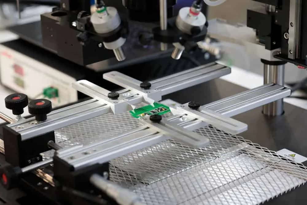
What AOI inspection actually does on a PCB assembly line
AOI uses cameras, lighting, image libraries, and measurement rules to compare the built board against expected component presence, polarity, position, and solder-joint appearance. In most SMT lines, AOI is placed after reflow and sometimes after print or placement, depending on the line configuration. The system is good at finding visible defects quickly across many boards with consistent logic.
That matters because the economics of assembly defects are brutal. A placement error found immediately after reflow can often be reworked in minutes. The same defect found after conformal coating, box build, or field return can cost 10 to 100 times more once labor, logistics, diagnosis, and schedule damage are included.
"On a stable SMT line, AOI should not be treated as a camera taking pictures. It is a feedback loop. If the false-call rate stays above about 15%, operators start bypassing alarms, and the inspection gate loses value fast."
— Hommer Zhao, Technical Director
In practice, AOI is strongest when it is connected to disciplined process setup. Library creation, golden board approval, component height rules, lighting recipes, and defect classification all need engineering ownership. Without that work, the machine may still generate results, but the results will not be reliable enough to support release decisions.
The defects AOI catches well
AOI is especially effective for visible, pattern-based defects on the assembled surface of the board. Common examples include:
- missing components
- wrong polarity on diodes, LEDs, or electrolytic capacitors
- tombstoning of passives
- skewed or shifted chip components
- insufficient or excessive visible solder on gull-wing leads
- solder bridges that are optically exposed
- wrong part size where the vision library can distinguish the geometry
- lifted leads on QFP and SOIC devices
For high-mix production, this matters because AOI gives a repeatable inspection baseline even when product variants change week to week. It is one reason many OEM teams expect AOI by default on custom PCB assembly and circuit board assembly services.
"AOI is excellent at the obvious defects that humans get tired of checking on the 200th board. Missing 0402 parts, polarity errors, and lead lift are exactly the kind of escapes that a tuned vision system should catch at near-100% repeatability."
— Hommer Zhao, Technical Director
Where AOI inspection is weak or incomplete
Buyers should be careful here. AOI sees what the camera can see. It does not directly verify hidden solder joints under BGAs, LGAs, bottom-terminated QFNs, or many shielded structures. It also does not prove electrical performance. A board can pass AOI and still fail in-circuit test or functional test because the defect is electrical rather than visually obvious.
AOI is also limited by reflectivity, shadowing, board warpage, inconsistent silkscreen, poor fiducial strategy, and library mistakes. If the supplier uses one generic recipe across many product families, nuisance alarms rise and real defects become easier to miss.
The most common blind spots are:
- hidden joints under BGA, LGA, and many QFN packages
- head-in-pillow or voiding conditions not visible from above
- wrong internal value on visually identical passive parts
- cold joints that still look cosmetically acceptable from the camera angle
- connector retention issues inside housings
- electrical opens or shorts that require net-level test
That is why AOI should be framed as a visible-surface inspection method, not a full quality guarantee. If your design uses hidden joints or high-reliability interfaces, you usually need BGA soldering service, X-ray, ICT, or functional test layered on top.
"The biggest buyer mistake is assuming AOI and X-ray are interchangeable. They are not. AOI inspects visible geometry; X-ray inspects hidden solder structures. On 0.5 mm BGA pitch, treating them as substitutes is how escapes reach the field."
— Hommer Zhao, Technical Director
AOI versus other PCB inspection methods
The fastest way to understand AOI is to compare it with the other gates around it.
| Inspection method | Best at catching | Main limitations | Typical use point | When buyers should insist on it |
|---|---|---|---|---|
| AOI | Missing parts, polarity, tombstones, exposed bridges, lead lift | Cannot see hidden joints or prove electrical behavior | After reflow, sometimes after placement | Standard SMT builds with visible joints and moderate complexity |
| SPI | Solder paste volume, area, offset, bridging before placement | Does not inspect final solder joints or wrong parts | After stencil printing | Fine-pitch SMT, 0.4 mm CSP/BGA, and new stencil programs |
| X-ray | Hidden joints, BGA voiding, opens under bottom-terminated packages | Slower, higher cost, interpretation still matters | After reflow on selected assemblies | BGA, LGA, QFN, BTC, dense power modules |
| ICT | Opens, shorts, wrong values, polarity, continuity at net level | Needs fixture access and stable revision | After assembly before shipment | Repeat production where electrical coverage matters |
| Functional test | Real operating behavior, firmware, interfaces, sensors | Slower and product-specific | End of line or system stage | Products where use-case behavior matters more than appearance |
| Visual inspection | Cosmetic review, workmanship context, odd one-off concerns | Operator fatigue and inconsistency | Manual checkpoints throughout build | Prototype runs, rework confirmation, customer-specific criteria |
In a mature process, these methods complement each other rather than compete. AOI is often the broad, fast screen. SPI reduces print-related escapes before parts are even placed. X-ray covers hidden solder joints. ICT and functional test catch electrical and behavioral failures that vision systems cannot.
How buyers should evaluate an AOI claim from a supplier
Many suppliers say they perform AOI. Fewer can explain the discipline behind it. When qualifying a supplier, ask practical questions:
- Is AOI performed on every assembled board or by sample?
- Is the inspection only post-reflow, or is there pre-reflow / post-print coverage too?
- How are golden boards approved and controlled by revision?
- What is the typical false-call rate after recipe tuning?
- Which package families are excluded or downgraded from AOI coverage?
- When does AOI trigger X-ray, ICT, or operator review rather than auto-release?
- Are defect pareto reports reviewed by engineering weekly or per lot?
A credible supplier should be able to answer these questions clearly. If the answer to everything is simply "we do 100% AOI," the quality system may be thinner than it sounds.
When AOI adds the most value in real production
AOI is most valuable on boards with enough visible SMT content to justify the programming effort and enough production repetition to benefit from trend data. It is especially useful when you are trying to reduce recurring defects such as polarity errors, missing passives, skew, solder bridging, or lifted gull-wing leads.
The value rises further when AOI data is used upstream. If a line shows a growing number of bridge calls on one device family, the right response may be stencil aperture adjustment, paste storage review, placement-force tuning, or reflow profile correction. AOI should shorten the time between defect creation and process correction.
For prototype work, AOI is still helpful, but buyers should be realistic. On the first build of a new design, engineering review, first-article confirmation, and direct technician feedback may matter as much as the machine result. That is why fast-turn and NPI programs often combine AOI with manual review and limited X-ray rather than relying on one gate.
Practical decision guide: when AOI alone is not enough
Use AOI as a baseline, but add more controls in these cases:
- BGA, LGA, QFN, or bottom-terminated packages: add X-ray because hidden joints are out of AOI view.
- Very fine-pitch SMT below 0.5 mm: add SPI because paste print quality drives many downstream defects.
- High-repeat production with net access: add ICT because electrical opens and wrong values can survive visual inspection.
- Medical, industrial, or safety-critical assemblies: add documented sampling plans, traceability, and release criteria linked to IPC acceptance rules.
- Boards with connectors, transformers, or mixed technology: add manual review or selective process checks where component geometry and solder mass vary significantly.
This layered approach is usually cheaper than a field failure. A supplier that understands that tradeoff is easier to trust than one promising that one machine does everything.
FAQ
Q: What defects can AOI inspection catch on a PCB assembly?
AOI is strongest at visible defects such as missing components, polarity errors, tombstoning, skew, exposed solder bridges, and lifted gull-wing leads. On a well-tuned SMT line, these categories can often be screened at near 100% board coverage, but the result still depends on recipe quality and package geometry.
Q: Can AOI inspection replace X-ray for BGA assemblies?
No. AOI cannot see most hidden solder joints under BGAs, LGAs, or many QFNs. For 0.4 mm to 0.8 mm pitch BGA work, X-ray is the correct complementary method because voiding, opens, and ball collapse issues are usually invisible from the top side.
Q: Is AOI enough for low-volume prototype PCB assembly?
Sometimes, but not always. For a first prototype run of 5 to 20 boards, AOI is useful for quick screening, yet engineering review and manual inspection still matter because the library and golden-board data are new. If the prototype includes hidden joints or critical power devices, add X-ray or bench test before release.
Q: What is the difference between AOI and SPI in SMT manufacturing?
SPI checks solder paste before placement, while AOI checks the assembled board after placement or reflow. SPI is especially valuable on fine-pitch apertures because a 20% paste-volume shift can create bridges or opens later, whereas AOI only sees the result after soldering.
Q: Should every PCB assembly lot receive 100% AOI?
Not automatically. For most modern SMT assemblies, 100% AOI is a sensible baseline, but the right answer depends on package mix, board complexity, and cost target. A connector-heavy or mixed-technology board may still need manual review, and a BGA-heavy board still needs X-ray on the hidden-joint population.
Q: How should buyers verify that a supplier's AOI program is credible?
Ask for the inspection scope, package exclusions, false-call handling, escalation rules, and examples of defect trend reports. A mature program should show revision-controlled recipes, operator verification, and a response plan when one defect category exceeds a threshold such as 10% to 15% nuisance calls or repeated escapes in the same lot.
Final takeaway
AOI inspection is an important control in PCB assembly because it catches many visible defects quickly and consistently. But it should be treated as one layer in a broader quality strategy, not as a standalone guarantee. Buyers get the best results when AOI is matched to the board technology, supported by disciplined recipe control, and combined with SPI, X-ray, ICT, or functional test when the product risk requires it.
If you want help defining the right inspection stack for your next PCB assembly program, contact our team. We can review your package mix, production volume, and reliability target to recommend the inspection gates that reduce real escape risk instead of just adding paperwork.
Related Articles


Need Help with Your PCB Design?
Check out our free calculators and tools for electronics engineers.
Browse PCB Tools"In over 20 years of manufacturing experience, we have learned that quality control at the component level determines 80% of field reliability. Every specification decision you make today affects warranty costs three years from now."
— Hommer Zhao, Founder & CEO, YourPCB