
Reflow Soldering vs Wave Soldering: Which Method Fits Your PCB Assembly?
Reflow soldering dominates SMT assembly while wave soldering remains the go-to for through-hole components. This guide breaks down the process differences, defect profiles, cost structures, and selection criteria so you can match the right method to your board design.
For more information on industry standards, see printed circuit board and IPC standards.
A contract manufacturer ran 10,000 mixed-technology boards through reflow only, skipping selective wave for the through-hole connectors. Field returns hit 8% within six months — cold joints on the power connectors caused intermittent failures under vibration. A second manufacturer used reflow for SMT components and selective wave for the through-hole leads on the same design. Field returns stayed below 0.3%. The difference was not skill or equipment quality. It was choosing the right soldering method for each component type.
Reflow soldering and wave soldering are the two dominant methods in PCB assembly, and picking the wrong one — or misapplying one where the other belongs — creates defects that surface months after shipping. This guide covers the process mechanics, defect profiles, cost structures, and decision criteria that determine which method fits your board.
How Reflow Soldering Works
Reflow soldering heats solder paste (a mixture of powdered solder alloy and flux) that has been pre-applied to PCB pads. The board passes through a reflow oven with four distinct thermal zones: preheat, thermal soak, reflow peak, and cooling.
During preheat (150–200°C over 60–120 seconds), the board temperature rises gradually to activate the flux and drive off volatile solvents. The thermal soak zone (150–200°C for 60–120 seconds) equalizes temperature across the board so that large thermal-mass components and small passives reach reflow temperature simultaneously. The reflow zone pushes the board above the solder's liquidus point — 217°C for SAC305 lead-free alloy or 183°C for Sn63/Pb37 leaded solder — for 30–60 seconds. Cooling at a controlled 2–4°C/second rate produces a fine-grained, mechanically strong joint.
"The thermal profile is the single most important variable in reflow soldering. A 5°C deviation at peak temperature can shift defect rates from 50 ppm to 500 ppm on fine-pitch QFP packages." — Hommer Zhao, Founder & CEO, WIRINGO
Stencil printing determines solder volume with high repeatability. A laser-cut stainless steel stencil — typically 0.10–0.15 mm thick for standard SMT — deposits paste onto each pad. Modern stencil printers achieve positioning accuracy within ±12.5 μm, which is critical for 0201-size components (0.6 mm × 0.3 mm) where excess paste causes bridging and insufficient paste causes open joints.
How Wave Soldering Works
Wave soldering passes the underside of a populated PCB across a standing wave of molten solder at 245–265°C. Components are inserted into through-holes and held by clinched leads or adhesive before the board enters the wave soldering machine.
The process follows three stages. First, flux is applied via spray or foam to the board's underside to remove oxides and promote wetting. Second, the board passes through a preheater (typically infrared) that raises the bottom-side temperature to 100–130°C, reducing thermal shock when the board contacts molten solder. Third, the board crosses the solder wave — usually a dual-wave system combining a turbulent "chip wave" (for SMT components glued to the bottom side) and a laminar "main wave" (for through-hole fill and smooth fillets).
Contact time with the wave is 2–4 seconds. Conveyor speed, wave height, board angle (typically 5–7° from horizontal), and solder temperature all interact to determine joint quality. A 1°C change in solder pot temperature affects viscosity and wetting behavior measurably.
Head-to-Head Comparison
| Parameter | Reflow Soldering | Wave Soldering |
|---|---|---|
| Primary use | SMT components | Through-hole components |
| Solder form | Paste (powder + flux) | Molten solder bath |
| Peak temperature | 230–250°C (lead-free) | 245–265°C (pot temp) |
| Contact time | 30–60 sec above liquidus | 2–4 sec in wave |
| Board sides soldered | Top and bottom (separate passes) | Bottom side only |
| Typical throughput | 100–200 boards/hour | 200–400 boards/hour |
| Capital cost (entry) | $15,000–$80,000 | $25,000–$120,000 |
| Solder waste | Low (paste is pre-metered) | Higher (dross from open bath) |
| Nitrogen option | Yes (reduces oxidation) | Yes (reduces dross 50–70%) |
| Best board density | High-density, fine-pitch | Low-to-medium density |
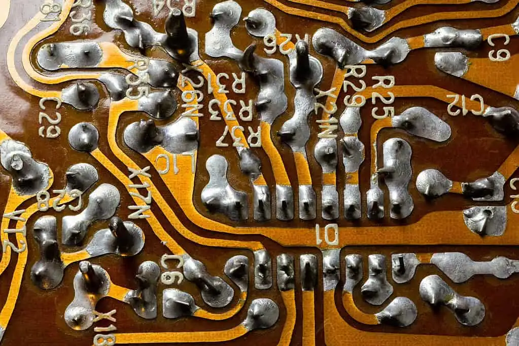
Defect Profiles: What Goes Wrong with Each Method
Reflow and wave soldering fail in different ways. Understanding the defect signature of each method helps you design boards that minimize rework.
Reflow soldering defects center on paste deposition and thermal profile errors. Tombstoning occurs when unequal pad sizes or uneven heating cause a passive component to stand upright on one end — IPC-A-610 Class 3 rejects boards with any tombstoned component. Head-in-pillow defects happen when the solder ball on a BGA partially melts but does not fully coalesce with the paste on the pad, creating a visually acceptable but electrically intermittent joint. Solder bridging between fine-pitch leads (below 0.5 mm pitch) results from excess paste volume or stencil misalignment.
Wave soldering defects concentrate on solder flow dynamics. Bridging between adjacent through-hole pins is the most common issue, caused by excessive solder wave height or incorrect board exit angle. Icicles (pointed solder protrusions) form when the board separates from the wave too slowly. Insufficient hole fill — where solder does not wick fully through the barrel — indicates inadequate flux activation, low preheat temperature, or excessive board thickness for the wave contact time.
"Wave soldering bridges are a physics problem, not a quality problem. Adjust the exit angle by 1–2 degrees and the conveyor speed by 5 cm/min before blaming the operator." — Hommer Zhao, Founder & CEO, WIRINGO
Cost Comparison: Materials, Setup, and Per-Board Economics
Cost differences between the two methods extend beyond equipment price.
Solder paste for reflow costs $80–$150 per 500g jar (SAC305 Type 4), and a standard board uses 0.5–2g of paste depending on component count. Wave solder bar costs $15–$25 per kg, but a 200 kg solder pot loses 1–3% to dross daily — that adds $3–$15 per day in material waste even when running nitrogen.
Stencils for reflow cost $150–$400 per design (laser-cut stainless steel) and last for 50,000+ prints. Wave soldering requires pallets or carriers for mixed-technology boards, costing $200–$800 per fixture, but these are reusable across production runs.
Energy costs differ significantly. A reflow oven consumes 8–15 kW continuously. A wave solder machine with preheater and pot heater draws 12–25 kW. For high-volume runs, wave soldering's faster cycle time (2–4 seconds vs. 4–6 minutes per board in the oven) offsets the higher power draw.
Per-board cost at volume (10,000+ units): reflow typically runs $0.02–$0.08 per solder joint; wave runs $0.01–$0.04 per joint. Wave is cheaper per joint but only applies to through-hole connections.
When to Use Reflow Soldering
Reflow soldering is the default for any board with surface-mount components — which covers over 90% of modern electronics. Use reflow when your design includes:
- Fine-pitch ICs (QFP, QFN, BGA packages with pitch below 0.65 mm) where solder volume precision matters
- High-density boards with 0402, 0201, or 01005 passives that require accurate trace widths and controlled solder deposition
- Double-sided SMT assemblies where components populate both sides of the board
- Temperature-sensitive components that benefit from a controlled, gradual thermal profile rather than sudden contact with a 255°C solder wave
- Lead-free processes where the narrow process window of SAC305 (liquidus 217–220°C, peak 235–250°C) demands tight thermal control
When to Use Wave Soldering
Wave soldering remains essential for through-hole technology and specific mixed-assembly scenarios:
- Through-hole connectors and terminals that require barrel fill per IPC-A-610 Class 2 (≥50% fill) or Class 3 (≥75% fill)
- High-power components (transformers, large electrolytic capacitors, relay sockets) that need the mechanical strength of a full through-hole solder fillet
- High-volume, low-mix production where conveyor speed and 2–4 second cycle times maximize throughput
- Bottom-side SMT components glued to the board and soldered in a single pass with through-hole parts using a dual-wave system
Mixed-Technology Assembly: Using Both Methods
Most modern boards combine SMT and through-hole components. The standard process flow for mixed-technology assembly is:
- Print solder paste on SMT pads (top side)
- Place SMT components via pick-and-place machine
- Reflow solder the top-side SMT assembly
- Flip the board and insert through-hole components
- Wave solder or selective solder the through-hole joints on the bottom side
Selective soldering — a targeted variant of wave soldering that uses a programmable nozzle to apply molten solder only to specific through-hole joints — has largely replaced full wave soldering in mixed-technology production. Selective soldering avoids thermal stress on nearby SMT joints and eliminates the need for solder pallets. Equipment cost runs $40,000–$150,000, positioned between reflow and full wave systems.
"For boards with fewer than 20 through-hole joints, selective soldering almost always beats wave soldering on total cost. You eliminate pallet costs and reduce solder waste by 80%." — Hommer Zhao, Founder & CEO, WIRINGO
Decision Matrix: Choosing the Right Method
Use this framework to match your board to the right soldering method:
| Decision Factor | Choose Reflow | Choose Wave | Choose Both |
|---|---|---|---|
| Component types | SMT only | THT only | Mixed SMT + THT |
| Board density | High (>15 components/cm²) | Low (<5 components/cm²) | Medium-high |
| Production volume | Any | High (>5,000/run) | Any |
| Fine-pitch ICs | Yes (BGA, QFN, <0.5mm pitch) | No | Yes (reflow side) |
| Mechanical strength needed | Standard | High (connectors, power) | Varies by component |
| Budget for equipment | $15K–$80K | $25K–$120K | $50K–$200K combined |
For prototype and low-volume runs, reflow with hand soldering of through-hole components often eliminates the need for wave soldering equipment entirely. This approach works well for quantities under 500 boards where the cost of a wave solder pallet cannot be amortized.
Industry Standards That Govern Both Methods
Both soldering methods must produce joints conforming to IPC-A-610 (Acceptability of Electronic Assemblies) and J-STD-001 (Requirements for Soldered Electrical and Electronic Assemblies). Key criteria include:
- Wetting angle: Below 90° for acceptable joints, below 45° preferred
- Fillet shape: Concave, smooth, and shiny (leaded) or slightly grainy (lead-free)
- Through-hole fill: ≥75% for Class 3 (high-reliability), ≥50% for Class 2
- Bridging: Zero tolerance across all classes
- Voiding: Below 25% for BGA joints per IPC-7095
Understanding these standards helps you set realistic quality expectations when selecting a soldering method and communicating requirements to your assembly partner.
References
- IPC-A-610 Standard — IPC Electronics Association
- Reflow Soldering Overview — Wikipedia: Reflow Soldering
- Wave Soldering Process — Wikipedia: Wave Soldering
- All About Circuits — Reflow vs Wave Comparison
Frequently Asked Questions
Which soldering method produces stronger joints — reflow or wave?
Wave soldering typically produces mechanically stronger joints on through-hole components because molten solder fills the entire plated barrel, creating a 360° fillet around the lead. For surface-mount joints, reflow produces reliable connections that meet IPC-A-610 Class 3 shear-strength requirements. The choice depends on whether your design needs mechanical retention (wave, for connectors under insertion force) or fine-pitch electrical reliability (reflow, for BGA and QFN packages).
Can I use reflow soldering for through-hole components?
Yes, through a technique called pin-in-paste (also known as intrusive reflow). Solder paste is printed into the through-hole pads with a modified stencil aperture, components are inserted, and the assembly goes through the reflow oven. Pin-in-paste works for components with 2–6 pins and moderate thermal mass, but it struggles with large connectors or components requiring >75% hole fill. IPC J-STD-001 provides criteria for acceptable pin-in-paste joints.
I'm designing a board with 200 SMT components and 8 through-hole connectors — what soldering approach should I use?
Reflow for the SMT assembly, followed by selective soldering for the 8 through-hole connectors. Selective soldering targets only the through-hole joints without affecting the already-reflowed SMT components. At 8 joints, a wave solder pallet is not cost-justified — you would spend $300–$800 on a pallet that selective soldering eliminates. This combination handles your impedance-sensitive signal paths and power connectors with the right method for each.
What is the biggest cause of defects in wave soldering?
Bridging between adjacent pins accounts for 40–60% of wave solder defects in most production environments. Root causes include: solder wave height set too high relative to board clearance, conveyor speed too slow (allowing excess solder adhesion), incorrect board exit angle, or insufficient flux activity. Adjusting the exit angle by 1–2° and optimizing conveyor speed typically reduces bridging by 70% or more without requiring new equipment.
How does lead-free solder affect the choice between reflow and wave?
Lead-free alloys like SAC305 (Sn96.5/Ag3.0/Cu0.5) have a liquidus temperature of 217–220°C versus 183°C for Sn63/Pb37, narrowing the process window for both methods. Reflow peak temperatures rise to 235–250°C, and wave solder pot temperatures increase to 255–265°C. The tighter process window makes reflow's precise thermal profiling more advantageous for fine-pitch components. Wave soldering with lead-free alloys generates more dross and requires more aggressive flux, increasing maintenance and material costs by 15–25%.
Does the choice of soldering method affect my PCB design?
Significantly. For reflow, pad design must follow IPC-7351 land pattern recommendations — oversized pads cause tombstoning, undersized pads cause insufficient fillets. For wave soldering, component orientation matters: orient all SMD components perpendicular to the wave direction and ensure consistent lead spacing to prevent bridging. Through-hole pad annular ring size affects capillary fill. Design for the soldering method early — retrofitting a layout for a different process adds 1–2 design revision cycles.
Choosing between reflow and wave soldering is an engineering decision, not a preference. Match the method to your component types, volume requirements, and reliability targets. For a design review that includes soldering method recommendations tailored to your board, contact us to discuss your project requirements.

Need Help with Your PCB Design?
Check out our free calculators and tools for electronics engineers.
Browse PCB Tools"In over 20 years of manufacturing experience, we have learned that quality control at the component level determines 80% of field reliability. Every specification decision you make today affects warranty costs three years from now."
— Hommer Zhao, Founder & CEO, WIRINGO