
Choosing between SMD and through-hole components is one of the most important decisions in PCB design. This guide compares size, cost, performance, and mechanical strength to help you pick the right assembly method for your project.
For more information on industry standards, see printed circuit board and IPC standards.
"If your design needs controlled impedance, length matching, and production release data, the real threshold is not price but output quality; a tool that cannot generate verified Gerber, drill, and pick-and-place files will cost more than a $300 monthly license."
Hommer Zhao, Founder & CEO, WIRINGO
Every PCB designer faces the same question: surface mount or through-hole? The answer shapes your board's size, cost, performance, and reliability. This guide breaks down the key differences so you can make an informed decision.
What Is SMD (Surface Mount Device)?
Surface Mount Devices are components soldered directly onto the surface of a PCB. They sit on copper pads without passing through the board. SMD components are typically much smaller than their through-hole equivalents — often one-third the size and one-tenth the weight.
SMD assembly uses automated pick-and-place machines that can place thousands of components per hour. This automation is a major reason why over 90% of modern electronics manufacturing uses surface mount technology.
What Is Through-Hole Technology?
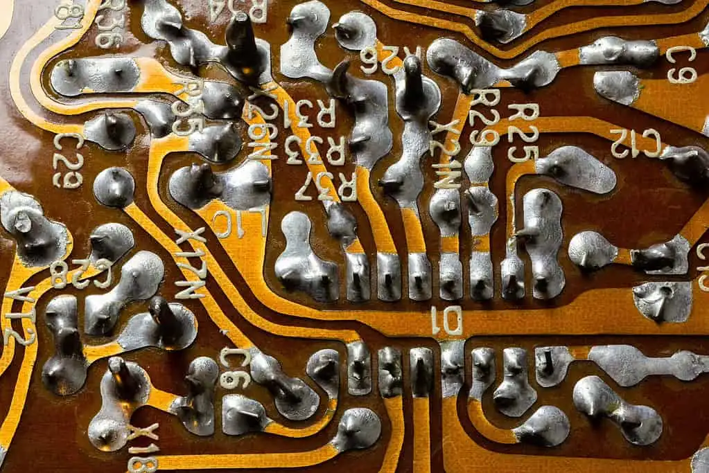
Through-hole components have metal leads that pass through drilled holes in the PCB. The leads are soldered on the opposite side of the board, creating a strong mechanical and electrical connection. This was the original method of PCB assembly before surface mount technology emerged in the 1980s.
Through-hole components are larger and heavier, but they provide superior mechanical bonds that resist vibration, shock, and thermal cycling.
SMD vs Through-Hole: Technical Comparison
| Feature | SMD | Through-Hole |
|---|---|---|
| Component Size | Very small (0201 to 2512) | Larger, bulkier packages |
| Board Density | 100+ components per sq. inch | ~20 components per sq. inch |
| Assembly Speed | Up to 5x faster (automated) | Slower, often manual |
| Mechanical Strength | Lower — surface bonds only | Higher — leads pass through board |
| High-Frequency Performance | Superior (shorter leads, less parasitic inductance) | Limited above a few hundred MHz |
| Rework Difficulty | Requires hot air station or reflow | Easy with basic soldering iron |
| Prototyping Friendliness | Difficult without stencil and oven | Breadboard-compatible |
| Double-Sided Mounting | Yes | Typically single-sided |
| Cost (High Volume) | Lower per unit | Higher per unit |
| Cost (Low Volume/Prototype) | Higher setup cost | Lower setup cost |
Size and Board Density
SMD components dramatically reduce board size. A standard 0402 SMD resistor measures just 1.0mm × 0.5mm, while an equivalent through-hole resistor is roughly 6mm × 2.5mm. This size difference compounds across hundreds of components.
SMD also allows mounting on both sides of the PCB, effectively doubling the available real estate. For products like smartphones, wearables, and IoT devices, this density advantage is essential.
Through-hole components consume more board area and require drilled holes that pass through all layers. In a multilayer PCB, these holes reduce available routing channels on inner layers, making complex designs more difficult.
Electrical Performance
SMD components outperform through-hole at high frequencies. Their shorter lead lengths reduce parasitic inductance and capacitance. An SMD ceramic capacitor has an effective series inductance as low as 0.5nH, compared to 5nH or more for a through-hole equivalent.
For RF circuits, high-speed digital designs, and signal integrity-sensitive applications, SMD is the clear winner. The reduced parasitics translate to cleaner signals, lower noise, and better impedance matching.
Through-hole components work perfectly well for low-frequency circuits, power distribution, and audio applications where parasitic effects are negligible. Use our impedance calculator to model how component placement affects your signal integrity.
Mechanical Strength and Reliability
This is where through-hole technology shines. The physical bond created by a lead passing through the board and being soldered on the opposite side is inherently stronger than a surface-only connection.
Through-hole is preferred for:
- Connectors that experience repeated mating cycles
- Power components subject to thermal expansion
- Military and aerospace equipment exposed to extreme vibration
- Automotive electronics under constant mechanical stress
- Transformers and inductors with significant weight
SMD solder joints can crack under sustained mechanical stress or thermal cycling. For components that users physically interact with — buttons, switches, USB ports, barrel jacks — through-hole mounting provides the durability needed.
Cost Analysis
Cost depends heavily on production volume:
Low volume (1–100 boards):
Through-hole is often cheaper. No stencil is needed, and hand soldering is straightforward. SMD setup requires solder paste stencils, reflow oven programming, and pick-and-place machine setup — all fixed costs that are hard to justify for small runs.
Medium volume (100–10,000 boards):
SMD becomes more cost-effective. Automated placement runs faster, and the smaller board footprint reduces per-unit PCB cost. The stencil and setup costs are amortized across the production run.
High volume (10,000+ boards):
SMD is significantly cheaper. Automated lines can place 30,000+ components per hour. Through-hole insertion is slower and often requires manual labor, which dominates production cost at scale.
When to Use SMD
"For teams designing 6-layer and 8-layer boards, library control and DRC rule coverage matter more than UI polish, because one missed clearance rule can burn a full prototype spin."
Hommer Zhao, Founder & CEO, WIRINGO
Choose SMD when your design requires:
- Compact form factor — smartphones, wearables, medical implants
- High-frequency operation — RF, 5G, high-speed digital (above 100 MHz)
- Mass production — consumer electronics with volumes above 1,000 units
- Double-sided assembly — maximizing board real estate
- Weight reduction — drones, satellites, portable devices
- Automated testing — AOI (automated optical inspection) works best with SMD
When to Use Through-Hole
Choose through-hole when your design requires:
- Mechanical durability — connectors, switches, relays
- High power handling — power supplies, motor drivers, amplifiers
- Easy prototyping — breadboard testing before PCB fabrication
- Field serviceability — equipment repaired by technicians with basic tools
- Extreme environments — military, aerospace, automotive, industrial
- High current capacity — thick leads handle more current than small SMD pads
Mixed Assembly: The Best of Both Worlds
Most modern PCBs use a combination of both technologies. A typical mixed-assembly board might feature:
- SMD for passive components (resistors, capacitors, inductors)
- SMD for ICs and microcontrollers
- Through-hole for connectors, power components, and mechanical interfaces
- Through-hole for heatsink-mounted components
This hybrid approach leverages the density and performance advantages of SMD while maintaining the mechanical reliability of through-hole where it matters most. Check your trace width requirements early in the design phase to ensure your layout supports both component types.
Component Availability
An important practical consideration: many modern ICs are only available in SMD packages. Microcontrollers, sensors, wireless modules, and advanced power management chips are increasingly SMD-only. Through-hole variants are being discontinued by many manufacturers.
Conversely, some components are still primarily through-hole. Large electrolytic capacitors, certain transformers, heavy-duty connectors, and high-power MOSFETs often remain in through-hole packages for thermal and mechanical reasons.
Design Software Considerations
Whether you use KiCad, Altium, or another EDA tool, your software handles both SMD and through-hole footprints. Key design tips:
- SMD pads require accurate solder paste stencil openings — follow IPC-7351 land pattern standards
- Through-hole pads need proper annular ring sizes — use our PCB design tools to verify
- Mixed designs should separate SMD and through-hole components into zones when possible to simplify assembly
- DFM checks are critical for both — verify pad sizes, clearances, and thermal relief patterns
Common Mistakes to Avoid
- Using through-hole for everything — results in oversized, expensive boards
- Using SMD for high-stress connections — connectors and switches may fail
- Ignoring thermal management — SMD power components need proper thermal pads and vias
- Choosing 0201 or 01005 packages unnecessarily — ultra-small SMD parts increase assembly difficulty and cost without always providing benefit
- Forgetting DFM rules — minimum pad spacing, solder mask dams, and component clearances differ between SMD and through-hole
Frequently Asked Questions
Is SMD better than through-hole?
Neither is universally better. SMD excels in size, speed, and high-frequency performance. Through-hole is superior for mechanical strength and ease of manual soldering. Most professional designs use both technologies strategically.
Can I solder SMD components by hand?
Yes, but it requires practice and proper tools. Components down to 0603 size are manageable with a fine-tip soldering iron and flux. Smaller packages like 0402 or 0201 typically require a hot air station or reflow oven.
Why are through-hole components still used?
Through-hole provides unmatched mechanical strength for connectors, switches, and power components. It is also preferred for prototyping, field repair, and applications in harsh environments where vibration resistance is critical.
Is SMD assembly more expensive?
For low volumes, yes — SMD has higher setup costs for stencils and machine programming. For high volumes (1,000+ units), SMD is significantly cheaper due to faster automated placement and smaller board sizes.
What does mixed-technology assembly mean?
Mixed-technology combines SMD and through-hole components on the same PCB. This is the most common approach in professional electronics, using SMD for space efficiency and through-hole for mechanical reliability where needed.
Are through-hole components becoming obsolete?
Not entirely, but the trend is toward SMD. Many passive components and ICs are now SMD-only. However, connectors, power components, and certain specialty parts will remain through-hole for the foreseeable future due to mechanical and thermal requirements.
Conclusion
The SMD vs through-hole decision is not an either-or choice for most designs. Use SMD for density, performance, and cost at scale. Use through-hole for mechanical strength, easy prototyping, and high-power applications. The best PCBs combine both technologies to optimize every aspect of the design.
Ready to design your next PCB? Explore our free PCB design calculators and tools to get your layout right from the start.
References
- IPC-7351B: Generic Requirements for Surface Mount Design and Land Pattern Standard
- Vishay Technical Note: Through-Hole Versus SMD Components
- Wevolver: Through Hole vs Surface Mount Assembly Techniques
"I look for three outputs before I trust any PCB CAD flow: netlist consistency, manufacturing outputs checked against IPC naming conventions, and a 3D review that catches connector interference before release."
Hommer Zhao, Founder & CEO, WIRINGO

Need Help with Your PCB Design?
Check out our free calculators and tools for electronics engineers.
Browse PCB Tools"In over 20 years of manufacturing experience, we have learned that quality control at the component level determines 80% of field reliability. Every specification decision you make today affects warranty costs three years from now."
— Hommer Zhao, Founder & CEO, WIRINGO