Wave Soldering PCB Assembly: Buyer Guide for Mixed Through-Hole Boards
Wave soldering can protect cost and schedule on connector-heavy PCB assemblies, but only when pallets, thermal limits, flux control, and IPC workmanship criteria are frozen before release.
For more information on industry standards, see printed circuit board and IPC standards.
Robotics rollouts are often organized as multi-PO programs with staged deliveries. The challenge is not only logistics. When one constrained PO carries schedule pressure, the manufacturing plan has to remove avoidable soldering delays before the buyer's robotics integration window closes.
Wave soldering PCB assembly is a soldering process where a populated board passes over a controlled solder wave so through-hole leads are soldered in one repeatable operation. Selective soldering is a programmable process that applies solder only to defined through-hole joints. A solder pallet is a fixture that shields SMT parts, controls board support, and exposes only the joints that should touch flux and solder. Through-hole technology is a component mounting method where leads pass through plated holes and are soldered on the opposite side.
TL;DR
- Use wave soldering when the board has many compatible through-hole joints and a stable pallet design.
- Use selective soldering when SMT parts, thermal mass, or keep-out areas make full-wave exposure risky.
- Freeze IPC-A-610 class, IPC-J-STD-001 soldering rules, pallet windows, flux type, and inspection evidence before quoting.
- Ask for first-article photos, solder-side inspection, thermal-sensitive component review, and defect reaction rules.
- Treat soldering method as a release decision, not a factory preference.
This guide is written for hardware engineers, sourcing managers, and NPI buyers who already have a mixed-technology board and must decide how the supplier will solder connectors, relays, transformers, terminal blocks, or other through-hole parts. I am writing from the role of a senior factory engineer with 18 years of PCB fabrication, SMT assembly, through-hole soldering, wire harness, cable assembly, and box-build program experience. The objective is to help buyers freeze the soldering method before the RFQ turns into a late production change.
Standards give the decision a shared language. IPC electronics standards provide the context for IPC-A-610 acceptability and IPC-J-STD-001 soldered electrical and electronic assembly requirements. Surface-mount technology explains why many mixed boards run SMT first, then through-hole soldering. Through-hole technology explains the mechanical anchoring that keeps large connectors and power parts in many designs.
Start With the Assembly Sequence
Most mixed-technology PCB assemblies follow a practical sequence: SMT paste print, pick-and-place, reflow, inspection, through-hole insertion, soldering, touch-up where allowed, cleaning if required, inspection, programming, and test. The soldering method belongs in the release package because it changes board layout, component selection, fixture cost, inspection points, and lead time.
For a connector-heavy robotics controller, a delayed soldering decision can turn into a schedule problem. If the factory quotes selective soldering and later finds that the board is better suited to a palletized wave process, the buyer may need a new fixture, new thermal review, and a fresh first article. If the factory assumes wave soldering and the board has bottom-side SMT too close to exposed windows, the result may be bridging, shadowing, or heat damage.
"For a mixed board, the soldering route should be locked before pilot release. If IPC-A-610 class, pallet exposure, and bottom-side keep-out are still open after SMT files are approved, the buyer is already carrying schedule risk."
— Hommer Zhao, Technical Director
For related service planning, compare through-hole PCB assembly, selective soldering PCB assembly, SMT PCB assembly, and circuit board assembly services. If the program also includes final wiring or enclosure work, review turnkey electronics manufacturing before the soldering method is frozen.
When Wave Soldering Fits the Board
Wave soldering works best when the board has a meaningful population of through-hole leads that can be exposed to a common soldering process. Typical candidates include pin headers, terminal blocks, large electrolytic capacitors, transformers, relays, power connectors, and board-edge interface parts. The process can be efficient because many joints are soldered in one pass instead of one nozzle movement at a time.
The buyer should still ask for constraints. Bottom-side SMT parts need enough distance from pallet windows. Tall parts need clearance through the machine. Heat-sensitive components need a thermal review. Large copper planes can pull heat away from the joint and create insufficient fill if the preheat and contact time are weak. Dense connector rows can create bridging if lead length, hole size, flux activity, solder temperature, or board angle is not controlled.
A good RFQ does not need to specify every machine parameter, but it should state what the factory must prove. Ask for the intended soldering method, pallet requirement, acceptance class, flux type, whether cleaning is required, and what first-article evidence will be provided.
When Selective Soldering Is the Better Route
Selective soldering is usually better when only a small number of through-hole joints need solder, when bottom-side SMT density is high, when keep-out areas are tight, or when certain components cannot tolerate wave exposure. It can also reduce fixture complexity on low-volume builds because the nozzle can be programmed around local areas.
The trade-off is cycle time and programming control. Selective soldering is not automatically safer just because it is local. The supplier still needs access for the nozzle, stable board support, correct fluxing, controlled dwell, and inspection rules for barrels that are hard to see. On heavy copper boards, a selective process may need more dwell time or local preheat, and that can affect nearby plastic bodies.
"Selective soldering is not a magic repair for a board with no soldering keep-out. I still want to see nozzle access, preheat evidence, and IPC-J-STD-001 process limits before I approve a pilot lot."
— Hommer Zhao, Technical Director
If the buyer is not sure which route fits, send the supplier the Gerbers, assembly drawing, BOM, XY data, bottom-side component map, and required IPC class. A responsible supplier should return a soldering recommendation with constraints, not only a price.
Wave vs Selective Soldering Decision Table
| Decision point | Wave soldering buyer check | Selective soldering buyer check | Practical release rule |
|---|---|---|---|
| Through-hole joint count | Best when many compatible joints can pass in one fixture | Best when the count is low or scattered | Above roughly 30 to 50 joints, compare fixture cost and cycle time |
| Bottom-side SMT | Needs pallet shielding and clear keep-out from exposed windows | Can avoid many bottom-side parts by path programming | Freeze bottom-side keep-out before layout release |
| Thermal mass | Needs preheat and contact time suitable for large copper areas | May need local dwell and nozzle tuning | Review heavy planes and high-current connectors before pilot |
| Component sensitivity | Risk rises for plastics, switches, relays, and shields near the wave | More local control but still needs heat review | Flag parts with low temperature limits in the BOM |
| Fixture need | Usually needs a solder pallet for mixed boards | May need simpler support fixtures | Quote fixture cost and fixture lead time separately |
| Inspection evidence | Solder-side photos, barrel fill review, bridge checks, pallet mark review | Joint photos, nozzle path approval, skipped-area review | Tie acceptance to IPC-A-610 Class 2 or Class 3 |
| Production volume | Strong fit for repeat lots after pallet approval | Strong fit for lower-volume or constrained geometry | Match method to annual volume, not only prototype convenience |
This table should be attached to the sourcing decision record. It prevents the team from choosing a method only because one supplier owns one machine type.
What Buyers Must Freeze Before Quoting
Freeze the soldering method early enough that the supplier can quote the real route. The minimum package should include Gerber files, drill data, BOM, XY placement file, assembly drawing, IPC class, expected quantity, revision status, bottom-side keep-out map, and any no-clean or cleaning requirement.
The drawing should name lead length limits where the component supplier allows it. Excessively long leads can drag solder and create bridges. Very short leads can reduce visible evidence and barrel fill confidence. If the assembly will use press-fit connectors, hand soldering, or staking on some parts, separate those steps from the wave or selective process so inspection records stay clean.
For higher-risk builds, ask for a first article package with at least solder-side photos of representative connector rows, inspection notes for any bridged or touched-up joints, pallet window photos, and confirmation that the board did not show heat damage. If X-ray, ICT, or functional test is also required, keep those gates separate from the visual soldering review. Related inspection decisions are covered in AOI inspection in PCB assembly, X-ray inspection in PCB assembly, and ICT vs functional test in PCB assembly.
Pallet, Flux, and Cleaning Controls
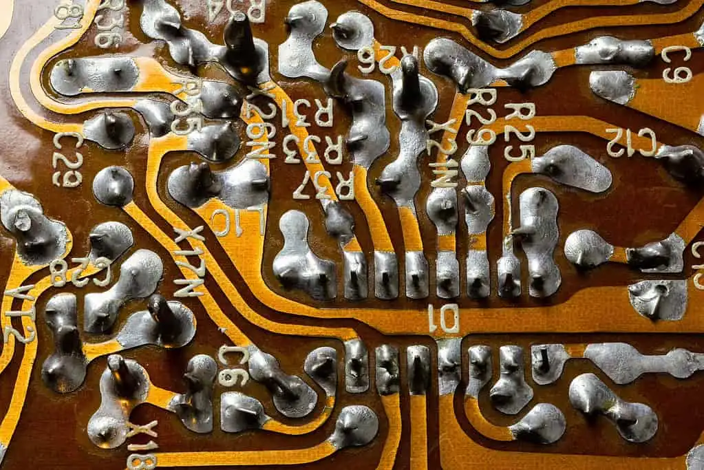
A wave solder pallet is part of the manufacturing process, not a generic accessory. It defines which solder joints are exposed, how the board is supported, where heat can reach bottom-side components, and how repeatable the pass will be. If the pallet is weak, the process can create defects even when the solder wave itself is stable.
Ask the supplier to identify pallet material, window locations, component clearance, expected fixture life, and whether the pallet can trap flux residue. For no-clean flux, the buyer should still define cosmetic and reliability expectations because visible residue around connectors, high-impedance nodes, or coating areas can become a release dispute. For cleanable flux, define cleaning method, drying rule, and whether ionic contamination testing is required. The related risk is discussed in PCB cleanliness and ionic contamination.
"A solder pallet controls more than masking. On a Class 2 or Class 3 assembly, it controls heat exposure, solder access, flux residue paths, and whether the same connector row can be inspected the same way every lot."
— Hommer Zhao, Technical Director
Do not approve a pilot plan that says only wave solder. Ask what is protected, what is exposed, what will be inspected, and what triggers process correction.
Weakest Section Rewrite: Replace Method Labels With Evidence
The weakest buyer note is usually: "Supplier will wave solder the connectors." Replace it with: "Supplier will run SMT reflow first, insert through-hole connectors after AOI, use a dedicated solder pallet exposing only connector rows J1 through J6, inspect solder-side joints to IPC-A-610 Class 2, control soldering workmanship to IPC-J-STD-001, photograph first-article joints, and document any touch-up before ICT."
That substitution changes the release decision. The first sentence names a machine. The second sentence defines sequence, fixture exposure, standards, evidence, and the next test gate. This kind of decision record is what keeps a multi-PO program from losing time when one PO already has schedule pressure.
Buyer Checklist Before Pilot Release
Use this checklist before approving a mixed through-hole PCBA build:
- The soldering route is named as wave, selective, hand soldering, press-fit, or a controlled combination.
- IPC-A-610 class and IPC-J-STD-001 process expectations are stated in the quote or quality plan.
- Bottom-side SMT keep-out and pallet windows have been reviewed against the actual layout.
- Heat-sensitive parts, plastic bodies, switches, relays, and shields have been reviewed before first article.
- Lead length, hole size, annular ring, and copper-plane effects are understood for high-mass joints.
- Flux type, cleaning rule, and residue expectations are defined before shipment.
- First-article evidence includes solder-side photos and a written disposition for any touch-up or bridge.
If one item is missing, keep the build in pilot status. A production release should not depend on discovering the soldering plan during the line walk.
FAQ
Q: When should buyers choose wave soldering for PCB assembly?
Choose wave soldering when a mixed board has many through-hole joints, enough bottom-side keep-out for pallet windows, and repeat volume that justifies fixture control. Ask for IPC-A-610 Class 2 or Class 3 acceptance, IPC-J-STD-001 workmanship control, and first-article solder-side evidence before volume release.
Q: Is selective soldering always better than wave soldering?
No. Selective soldering can be better for tight geometry or low through-hole count, but it may be slower on boards with 30 to 50 or more compatible joints. The right choice depends on nozzle access, thermal mass, bottom-side SMT, fixture cost, and required inspection evidence.
Q: What files does a supplier need to judge wave soldering feasibility?
Send Gerbers, drill files, BOM, XY placement data, assembly drawing, bottom-side component map, expected volume, IPC class, and cleaning requirement. Without those files, the supplier cannot judge pallet windows, thermal exposure, lead length risk, or inspection access with enough confidence.
Q: What defects should buyers watch for after wave soldering?
Common wave-solder defects include bridges, insufficient barrel fill, icicles, skipped joints, disturbed joints, overheated plastic bodies, flux residue traps, and solder balls. The first article should include solder-side photos and a defect reaction plan before the build moves beyond pilot.
Q: Can wave soldering be used after SMT reflow?
Yes. Many mixed-technology PCB assemblies run SMT reflow first, then through-hole insertion and wave soldering. The buyer must protect bottom-side SMT parts with pallet design, confirm keep-out, and define inspection to IPC-A-610 before approving repeat production.
Q: How does wave soldering affect PCBA delivery schedule?
Wave soldering can shorten repeat-lot cycle time after the pallet is approved, but the first build may need fixture design, thermal review, first-article inspection, and touch-up rules. For split PO programs, quote the pallet lead time separately so one constrained shipment does not surprise the buyer.
Final Takeaway
Wave soldering is a strong option for mixed through-hole PCB assembly when the board layout, pallet design, flux control, thermal exposure, and IPC acceptance criteria are locked before pilot release. Selective soldering remains the better route when geometry is constrained or local heat control is the main risk. Buyers get the best outcome when they treat the soldering method as a documented manufacturing decision with evidence, not as a late factory choice.
YourPCB supports SMT, through-hole, selective soldering, wave soldering planning, inspection, and test for mixed electronics assemblies. To review a mixed-technology board before pilot release, contact YourPCB.


Need Help with Your PCB Design?
Check out our free calculators and tools for electronics engineers.
Browse PCB Tools"In over 20 years of manufacturing experience, we have learned that quality control at the component level determines 80% of field reliability. Every specification decision you make today affects warranty costs three years from now."
— Hommer Zhao, Founder & CEO, YourPCB