Through-Hole PCB Assembly Services
Professional through-hole PCB assembly with wave soldering and selective soldering capabilities. IPC-A-610 Class 3 compliant, SAC305 lead-free processing, hole fill rates exceeding 90%, and lead times from 5 business days for prototype quantities.

Why Through-Hole Assembly Still Matters
Surface mount technology dominates modern PCB assembly, but through-hole technology (THT) remains essential for specific applications where mechanical strength, current carrying capacity, or serviceability are non-negotiable. A power connector soldered only to surface pads will fail under repeated mating cycles. A transformer delivering 10A needs leads anchored through the board. These are engineering realities, not preferences.
The key decision point is straightforward: if a component experiences mechanical load, thermal cycling above 105°C, or current above 5A per pin, through-hole mounting is the reliable choice. For everything else, SMT is faster and cheaper. Most real-world boards are mixed technology, and managing that transition well is what separates a good assembly partner from a problematic one.
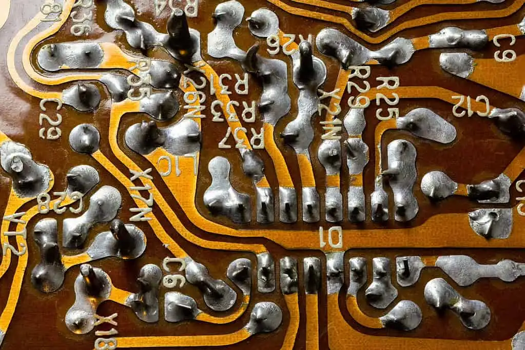
According to the IPC-A-610J standard, through-hole solder joints must achieve a minimum of 75% vertical hole fill for Class 2 and 75% for Class 3 assemblies, with wetting on the opposite side visible. These are the benchmarks we build to on every board.
Core Capabilities
🌊
Wave Soldering
Dual-wave (turbulent + laminar) soldering for pure through-hole or simple mixed boards. Supports board widths up to 400mm with conveyor speeds of 1.0-2.5 m/min. Ideal for high-volume production where throughput matters.
🎯
Selective Soldering
Programmable nozzle-based soldering for mixed-technology boards where SMT components on the bottom side preclude wave soldering. Pin-to-pin accuracy of ±0.5mm with nitrogen inerting for consistent wetting.
🔧
Hand Soldering
Skilled operators for low-volume, high-complexity, or rework tasks. Temperature-controlled stations with JBC and Metcal irons. Required for components incompatible with wave or selective processes, such as heat-sensitive devices.
⚡
Mixed Technology Assembly
SMT placement and reflow followed by through-hole soldering in a single workflow. We manage the thermal profile sequencing to prevent rework on SMT joints during the THT phase. This is the most common production scenario we handle.
🔍
Lead-Free RoHS Processing
SAC305 (Sn96.5/Ag3.0/Cu0.5) lead-free soldering compliant with EU RoHS Directive 2011/65/EU. We also support Sn63/Pb37 leaded processing for applications covered by RoHS Annex III exemptions, with JEDEC J-STD-609 marking.
📋
IPC Class 3 Inspection
Visual inspection to IPC-A-610J Class 1, 2, or 3 as required. AOI for SMT joints and manual inspection with 10x-40x stereo microscopes for through-hole solder quality. Full traceability with date codes and lot tracking.
Through-Hole Assembly Specifications
These are the parameters that actually affect your board's reliability and yield. Hole fill percentage directly correlates with joint strength. Solder alloy choice determines reflow temperature and long-term reliability under thermal cycling. Knowing these numbers upfront lets you design for manufacturability rather than discovering problems at prototype stage.
| Parameter | IPC Standard | Our Capability | Industry Benchmark |
|---|---|---|---|
| Vertical Hole Fill (Class 3) | ≥75% (IPC-A-610J) | ≥90% typical | 75-85% |
| Solder Alloy (Lead-Free) | SAC305 per J-STD-006 | SAC305 + Sn63/Pb37 | SAC305 only |
| Wave Solder Width Capacity | N/A | Up to 400mm | 300-350mm |
| Selective Solder Accuracy | N/A | ±0.5mm pin-to-pin | ±0.8mm |
| Board Thickness Range | 0.8-3.2mm typical | 0.6-4.0mm | 0.8-3.2mm |
| Component Lead Pitch (min) | 1.27mm DIP standard | 0.95mm (selective) | 1.27mm |
| Inspection Level | Sample per AQL | Visual + AOI per inspection plan | AQL sampling |
| Lead Time (Prototype) | N/A | 5-7 business days | 7-14 business days |
Through-Hole Assembly Process
The process differs depending on whether your board is pure through-hole or mixed technology. Here is the workflow for a typical mixed-technology board, which accounts for roughly 80% of the through-hole assemblies we produce.
1
Design Review & DFM Check
We review your Gerber files, BOM, and assembly drawings for through-hole specific issues: pad-to-hole ratio (ideally 1.5:1 to 2:1 for wave soldering), component spacing for selective solder nozzle access, and thermal relief patterns on ground planes. Catches at this stage prevent 60-70% of assembly defects downstream.
2
SMT Placement & Reflow (If Mixed Technology)
For mixed boards, SMT components are placed and reflowed first. The reflow profile is established per J-STD-020 for moisture-sensitive components. After reflow, AOI verifies SMT joint quality before the board moves to the through-hole stage.
3
Through-Hole Component Insertion
Components are inserted manually or with automated axial/radial sequencers depending on volume. Lead clinching secures components before soldering. For wave soldering, a flux application step precedes preheat. For selective soldering, flux is applied only to target joints via precision spray or drop-jet.
4
Soldering (Wave, Selective, or Hand)
Wave soldering: the board passes over a dual-wave solder pot at 255-265°C (lead-free) with nitrogen inerting. Selective soldering: a programmable nozzle solders each through-hole joint individually. Hand soldering: used for rework, low-volume, or components that cannot tolerate the wave or selective process temperatures.
5
Cleaning & Inspection
Post-solder cleaning removes flux residues using aqueous or solvent-based systems, critical for conformal coating adhesion and preventing electrochemical migration. Visual inspection under magnification checks hole fill, wetting, solder bridges, and cold joints per IPC-A-610J criteria.
6
Functional Testing & Shipment
ICT, flying probe, or custom functional testing verifies electrical integrity. Test reports document pass/fail results with serial traceability. Boards are packaged in ESD-safe materials with moisture barrier bags for MSL-rated components, ready for your incoming inspection.
Wave Soldering vs. Selective Soldering: When to Use Each
This is the most common question we get from engineers designing mixed-technology boards. The answer depends on your board layout, not your preference. If you have SMT components on the bottom side, wave soldering will destroy them unless you use expensive masking or pallets. Selective soldering avoids this entirely but is slower and costs more per joint.
Use Wave Soldering When:
- Board is pure through-hole or has no bottom-side SMT
- Production volume exceeds 500 boards per run
- Component density is uniform across the board
- Cost per joint is the primary driver (wave is 3-5x faster)
- Board width is under 350mm with standard component heights
Use Selective Soldering When:
- Bottom-side SMT components are present (most common scenario)
- Board has high-value components that cannot risk wave exposure
- Through-hole components are clustered in specific areas
- Lead pitch is below 1.27mm (selective handles down to 0.95mm)
- Low to medium volume where pallet tooling cost is not justified
In practice, roughly 70% of the mixed-technology boards we assemble use selective soldering. The remaining 30% are either pure through-hole (wave) or have simple bottom-side layouts that work with wave pallets. If you are unsure, send us your layout and we will recommend the approach that gives you the best yield at the lowest cost.
Case Study: Industrial Power Supply Mixed-Technology Assembly
Challenge
A power supply OEM needed 2,000 boards per month with 47 SMT components on the top side, 12 SMT components on the bottom side, and 23 through-hole components including a 15A transformer, high-current electrolytic capacitors, and a 9-pin D-sub connector. Their previous supplier had a recurring defect rate on through-hole joints due to insufficient hole fill on the transformer pins.
Solution
We implemented a two-stage process: SMT reflow first, then selective soldering for all through-hole components using a 6mm nozzle with nitrogen inerting. For the transformer pins (1.2mm lead diameter in 1.5mm holes), we increased preheat dwell time by 15 seconds and adjusted solder dip depth to 8mm above the board surface. DFM review also identified and corrected two pad-to-hole ratios that were below 1.5:1.
Results
Through-hole defects dropped sharply within the first production run, and hole fill on the transformer pins consistently met the IPC vertical-fill requirement. Rework stations were eliminated, which cut per-board assembly cost and shortened lead time from weeks to days.
Through-Hole Components We Assemble
Not all through-hole components are created equal. A DIP IC requires different handling than a 15A terminal block. Here is what we process regularly, along with the specific considerations for each type.
Connectors & Headers
- D-sub (9/15/25/37 pin), DB and HD variants
- Terminal blocks (screw, spring, pluggable) up to 30A
- Pin headers and socket strips (2.54mm, 2.0mm, 1.27mm pitch)
- MIL-SPEC circular connectors (MIL-DTL-38999, MIL-DTL-5015)
- USB, RJ45, and audio jacks with through-hole mounting tabs
Power & Passive Components
- Electrolytic and film capacitors (radial and axial)
- Power transformers and inductors (up to 500W)
- Axial and radial leaded resistors
- Relays (DPDT, SPDT, 4PDT) with 5-16A contact ratings
- Fuse holders and fuse clips
Semiconductors
- DIP ICs (6-48 pin), including OTP and windowed EPROMs
- TO-220, TO-247, TO-3 power packages
- Bridge rectifiers (KBP, KBU, KBPC series)
- TO-92 small-signal transistors and voltage regulators
- Optocouplers (DIP-4, DIP-6, DIP-8 packages)
Electromechanical
- DIP switches (piano, rotary, slide)
- Tactile and push-button switches
- Potentiometers and trimmers (single and multi-turn)
- Buzzers and transducers
- LEDs with through-hole mounting (3mm, 5mm, 10mm)
Industries That Rely on Through-Hole Assembly
Through-hole assembly is not a legacy technology. It is the correct technology for specific engineering requirements. These are the sectors where we see consistent demand:
- Industrial Power Electronics: Motor drives, inverters, and power supplies where components carry 10-50A and experience vibration and thermal cycling
- Aerospace & Defense: Avionics and ground support equipment requiring MIL-SPEC connectors and Class 3 inspection per IPC-A-610J
- Medical Devices: Patient-connected equipment where connector reliability is safety-critical and FDA traceability is mandatory
- Automotive: Engine control units and body electronics subject to vibration profiles per SAE J1455 and thermal shock cycling
- Test & Measurement: Precision instruments with BNC connectors, banana jacks, and high-voltage components requiring robust mechanical attachment
- Energy & Renewables: Solar inverters, battery management systems, and grid-tied equipment with high-current terminal blocks
Frequently Asked Questions
When should I choose through-hole assembly over surface mount?
Choose through-hole assembly for components that experience high mechanical stress (connectors, transformers, large capacitors), high-current paths above 5A, or when the board requires repeated mating cycles. Through-hole leads anchor through the board and are clinched on the opposite side, providing 3-5x the pull-out strength of SMT solder joints per IPC-A-610.
What is the minimum order quantity for through-hole PCB assembly?
Our MOQ starts at 5 boards for through-hole assembly. Prototype quantities of 5-20 boards typically ship in 5-7 business days. For production volumes of 100+ boards, lead time is 2-3 weeks depending on component availability and board complexity.
What files do I need to provide for through-hole assembly?
You need Gerber files (all layers), a BOM with manufacturer part numbers, pick-and-place or centroid data, assembly drawings showing component orientation, and any special soldering requirements. We accept Altium, KiCad, Eagle, and OrCAD native files as well.
What is the difference between wave soldering and selective soldering for through-hole components?
Wave soldering passes the entire bottom of the board over a molten solder wave, ideal for pure through-hole or simple mixed boards. Selective soldering uses a programmable nozzle to solder individual joints, necessary when SMT components on the bottom side would be damaged by the wave. Selective soldering adds roughly 15-20% to processing cost but is required for most mixed-technology boards.
Do you support lead-free through-hole assembly for RoHS compliance?
Yes, we process both Sn63/Pb37 leaded and SAC305 (Sn96.5/Ag3.0/Cu0.5) lead-free solder alloys. Lead-free wave soldering operates at 255-265°C versus 245-255°C for leaded. We also support backward-compatible assembly for exempt applications per RoHS Annex III.
What inspection standards apply to through-hole solder joints?
All through-hole solder joints are inspected to IPC-A-610J, the industry standard for acceptability of electronic assemblies. We offer Class 1, 2, and 3 inspection levels. Class 3 (used for aerospace and medical) requires 75% vertical hole fill minimum, while Class 2 requires 75% vertical fill with some exceptions per Table 7-1 of the standard.
Can you assemble mixed technology boards with both SMT and through-hole components?
Yes, mixed-technology assembly is our most common through-hole workflow. We place and reflow SMT components first, then solder through-hole components using selective soldering or hand soldering. This avoids thermal damage to SMT joints and maintains IPC-A-610 compliance for both technologies on the same board.
Related Services
SMT PCB Assembly
High-precision surface mount technology assembly for fine-pitch components, BGA, QFN, and 0201 chip placement.
Selective Soldering PCB Assembly
Use this path when mixed SMT/THT boards need localized connector soldering and bottom-side SMT protection.
Wave Soldering PCB Assembly
Use this path when through-hole or simple mixed boards need pallet review, flux control, and repeatable solder release.
PCB Assembly Prototype
Rapid prototype PCB assembly with turnkey component sourcing, from design files to tested boards in 5 days.
Wire Harness Contract Manufacturing
Full-service wire harness production for high-mix, low-volume programs with IPC-A-620 compliance.
Low Volume Wire Harness
Prototype and small-batch wire harness assembly with MOQ 1, ideal for engineering validation and pilot runs.
Get Your Through-Hole Assembly Quote
Send us your Gerber files and BOM. We will review your design for through-hole manufacturability and return a detailed quote within 24 hours, including our DFM recommendations.
Reviewed by: Engineering Team, YourPCB | Last updated: 2026-04-15

Backed by our Shenzhen SMT factory
26 placement machines · 11 SMT lines
4 nitrogen reflow ovens
100% 3D SPI & AOI inspection
Per-board MES traceability
01005 & PoP in stable production