How to Panelize a PCB: V-Scoring, Tab Routing, Rails & Fiducials Guide
PCB panelization is the difference between a board that assembles cleanly and one that breaks rails, scraps panels, or damages edge components. This guide explains when to use V-scoring vs tab routing, how to size rails and fiducials, and what to check before sending Gerbers to fabrication.
A PCB can pass bare-board fabrication and still fail on the SMT line because the panel was specified poorly. IPC-2221 gives the general design framework, but assembly details decide whether the panel survives handling, stencil printing, placement, reflow, and depaneling. JLCPCB's April 24, 2025 SMT guideline is a good reality check: for its assembly line, it recommends 5 mm process edges, 2 mm tooling holes, and 1 mm fiducials placed 3.85 mm from the panel edge. Those numbers explain why panelization is not paperwork. It is manufacturing design.
One engineering team lets the factory improvise the panel after layout is done. Components end up too close to the score line, the rails flex during transport, and operators hand-rework panels that should have run automatically. Another team plans the panel before Gerber release, leaves assembly clearance, and chooses the right breakaway method for the board shape. Same circuit. Very different yield.
This guide covers what PCB panelization is, when you should define it yourself, how to choose between V-scoring and tab routing, what to do with rails and fiducials, and the mistakes that create depaneling damage, placement errors, and avoidable cost.

What PCB panelization actually does
PCB panelization groups multiple boards into one larger manufacturing panel so fabrication and assembly equipment can process them efficiently. Instead of handling ten small boards one by one, the factory handles one rigid panel with repeatable geometry, tooling features, and enough edge area for conveyors, fiducials, and clamping.
That sounds simple, but panelization controls three things at once: mechanical stability, assembly compatibility, and cost per good board. A panel that is too weak can crack rails or warp in reflow. A panel with poor fiducial placement can hurt pick-and-place alignment. A panel that wastes material can quietly raise unit cost even when the circuit itself is fine.
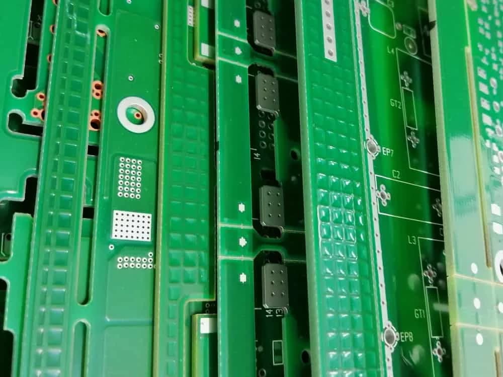
The useful way to think about it is the handling envelope: everything outside the board outline that exists only to help machines build your product. Rails, tooling holes, fiducials, tabs, score lines, coupons, and depanel clearances all belong to that envelope.
Should you let the fabricator panelize the board or define it yourself?
If your board is rectangular, has generous edge clearance, and has no unusual assembly constraints, letting the fabricator panelize it is often the fastest route. Many shops can optimize the array for their stock panel sizes and depaneling process better than a first-pass customer design can.
You should define the panel yourself when the board has edge-mounted connectors, castellations, irregular outlines, mouse-bite sensitivity, fine-pitch BGAs near the edge, or strict mechanical orientation requirements. In those cases, panelization affects solder quality and depanel stress directly, so leaving it unspecified invites re-interpretation.
Expert Insight — Hommer Zhao: "If the panel method changes the clearance to your connectors or edge components, it is no longer a CAM detail. It is part of the product design and should be reviewed before Gerber release."
A practical compromise works well on many jobs: send the individual board plus a proposed panel drawing, then ask the factory to confirm or improve it. That keeps manufacturing freedom where it helps, but protects the design intent where it matters.
The four panel features that matter most
A manufacturable panel usually comes down to four structural features: rails, tooling holes, fiducials, and breakaway boundaries. Ignore any one of them and the rest of the panel becomes harder to run.
Rails and process edges
Rails are non-functional strips added around the array so conveyors, clamps, and depanel fixtures can grip the panel without touching components. For automated SMT lines, rail width is not cosmetic. It is the buffer that keeps edge components away from guide hardware and gives room for fiducials and tooling holes.
JLCPCB's published SMT recommendation of 5 mm process edges is a useful baseline because it reflects real assembly equipment constraints, not textbook theory. Some factories want more, some can run less, but rails narrower than the assembly line can tolerate create the edge-collision trap: the board is technically buildable, yet components near the edge get scraped, shadowed, or reworked.
If your design has USB, board-edge terminals, or overhanging tall parts, call that out before the panel is finalized. The rail is there to protect the product, not just to satisfy a checklist.
Tooling holes
Tooling holes give assembly equipment fixed registration points for fixtures, stencils, and support tooling. They are mechanical references, not electrical features, so they should sit in the rails or dedicated panel frame instead of inside the functional board whenever possible.
A common published starting point is 2 mm tooling holes on the process edge for SMT assembly. What matters more than the exact diameter is consistency: the hole size, plating choice, and location must match the fixture plan used by the assembler. Randomly placed holes are almost as useless as having none at all.
If the board is thin, heavy, or asymmetrically populated, tooling support becomes more important because the panel is already more likely to flex. In those builds, ask where the assembler wants support pins before you lock the panel drawing.
Fiducials
Fiducials are optical reference marks used by pick-and-place and AOI systems. Global fiducials align the whole panel. Local fiducials help align dense or fine-pitch areas on individual boards.
A practical assembly baseline is three global fiducials on the panel frame and local fiducials when you have packages like BGAs, QFNs, or very fine-pitch components that cannot tolerate placement drift. JLCPCB's guideline also calls for 1 mm fiducials placed 3.85 mm from the panel edge, which is useful because it ties fiducial geometry to actual machine clearance.
Keep fiducials out of breakaway tabs, score lines, and copper clutter. A fiducial that sits too close to a routed edge, silkscreen, or exposed copper pour loses contrast and becomes harder for vision systems to read consistently.
Breakaway boundaries
The breakaway boundary is the planned separation method between boards: V-score, tab routing, or a hybrid. This boundary controls how much stress reaches the finished board when the array is separated.
Designers often focus on whether the board can be fabricated and forget to ask how it will be removed from the panel without damaging ceramic capacitors, loosening connectors, or whitening FR-4 near the edge. That is why breakaway planning has to happen before placement is frozen, not after.
V-scoring vs tab routing
The short answer is simple: use V-scoring for straight-edged rectangular boards that can tolerate a continuous score line, and use tab routing for irregular outlines, edge components, or boards that need more separation control.
The trade-off is not just geometry. It is speed vs flexibility. V-scoring is faster and usually cheaper because the cutter runs continuous lines across the panel. Tab routing is slower but handles shapes and edge conditions that scoring physically cannot.
A Reddit discussion from an engineer reviewing a fabrication drawing shows the classic mistake clearly: the user expected internal partial V-cuts, while experienced responders pointed out that V-grooves must run through to the panel extents. That is the kind of misunderstanding that produces a "looks right" panel file and a wrong finished panel.
| Method | Best For | Strengths | Risks | Typical Use Case |
|---|---|---|---|---|
| V-scoring | Rectangular arrays with straight separation lines | Low cost, fast production, clean edges | Sends stress through the full score line, not suitable for irregular outlines or edge parts near the score | Simple 2-layer or 4-layer consumer boards |
| Tab routing with mouse bites | Irregular outlines, rounded boards, edge connectors | Flexible geometry, better for complex shapes, easier to isolate stress | Leaves tab nubs that may need sanding or careful cleanup | Wearables, odd-shaped modules, connector-heavy boards |
| Hybrid panel | Mostly rectangular boards with selected routed features | Balances cost and geometry | More coordination required with the factory | Boards with straight outer edges but special internal cutouts |
Expert Insight — Hommer Zhao: "The cheapest depanel method is the one that does not crack your MLCCs after separation. A V-score that saves a few dollars is expensive if it creates latent field failures."
A practical panelization spec you can hand to a factory
The easiest way to avoid panelization ambiguity is to define a compact spec sheet with the items the CAM team actually needs. Even when the factory adjusts dimensions for its own process, this list shows your intent and surfaces conflicts early.
| Item | Good Starting Point | Why It Matters |
|---|---|---|
| Process edge / rail width | 5 mm if your assembler recommends it | Protects edge components and creates room for fiducials and tooling |
| Tooling holes | 2 mm in rails | Supports fixture alignment and repeatable registration |
| Global fiducials | 3 on the panel frame | Helps align the entire panel during placement and AOI |
| Local fiducials | Add for BGA or fine-pitch areas | Improves placement accuracy on dense boards |
| Breakaway method | V-score for straight lines, tabs for complex shapes | Controls cost, stress, and edge quality |
| Edge-component keepout | Define explicitly in fabrication notes | Prevents depanel damage and guide-rail collisions |
| Panel orientation | Mark top side and array direction | Avoids mirrored or rotated assembly surprises |
| Support requirements | Flag thin boards, heavy parts, or asymmetry | Reduces flex and warpage during reflow |
Before release, review the panel with the same seriousness you give to your PCB DFM rules. The panel is a manufacturing drawing, not an afterthought.
The panelization mistakes that scrap good boards
Most panelization failures are not exotic. They come from ordinary omissions that compound during assembly.
Mistake 1: components too close to the break line. Ceramic capacitors, board-edge connectors, and tall electrolytics all dislike flex. If they sit next to a score line or mouse-bite tab, the stress of separation can crack solder joints or damage the board edge.
Mistake 2: no plan for panel stiffness. A long, narrow panel with heavy components on one side is more likely to sag in reflow. That can distort placement and solder quality even if the bare board dimensions are in tolerance.
Mistake 3: treating fiducials as decoration. Poor contrast, bad spacing, or placing fiducials inside unstable tab areas makes machine vision less reliable. The board may still run, but not with the repeatability you expect.
Mistake 4: assuming the fab drawing means the same thing to everyone. Community threads on Reddit and KiCad forums repeatedly show the same pain point: engineers think the separator line will behave one way, but the factory interprets the file according to its house process. That is why notes, panel drawings, and confirmation screenshots matter.
How panelization affects cost more than most teams expect
Panelization affects cost through material utilization, assembly speed, and yield loss. Engineers often focus only on the first factor and miss the other two.
A denser array may look cheaper on paper because it fits more boards into one manufacturing panel. But if the depanel method slows handling, increases support tooling, or raises breakage risk, the true cost per shipped board can go up. This is the panel economics loop: cheaper geometry at fabrication can become more expensive geometry at assembly.
The opposite is also true. Adding rails or choosing tab routing may slightly increase raw panel area, yet reduce placement issues and depanel damage enough to lower final cost. That is why panel decisions should be judged on shipped yield, not only on square inches of laminate.
If the design includes controlled impedance or dense routing near the edge, review the panel and the board together. Your impedance calculator and PCB stackup planning are only part of the story if the finished panel warps or cracks during assembly.
A release workflow that catches panel problems early
A strong panelization workflow starts before Gerbers go out. Once component placement and edge geometry are frozen, panel options narrow quickly.
- Confirm whether the assembler or fabricator wants to own the final panel drawing.
- Mark board-edge keepouts for connectors, test pads, and fragile components.
- Choose the provisional breakaway method based on shape and stress tolerance.
- Add rails, tooling holes, fiducials, and orientation notes to the panel concept.
- Review copper balance, asymmetrical population, and likely support points.
- Generate manufacturing outputs and inspect them in a Gerber viewer before release.
- Ask the supplier to confirm any assumptions in writing before production starts.
For more general design hygiene, pair this with our guides on PCB via types and PCB surface finish selection. Panelization problems often show up alongside broader DFM mistakes, not in isolation.
References
- JLCPCB Help Center: Specifications for Adding Process Edges and Positioning Holes
- IPC-2221 Generic Standard on Printed Board Design (PDF mirror)
- Reddit discussion: first-time PCB fabrication and V-cut interpretation
- Reddit discussion: panelization guidelines from practicing designers
Frequently Asked Questions
What is the best PCB panelization method for a rectangular board?
For a simple rectangular board with straight separation lines and adequate edge clearance, V-scoring is usually the best starting point. It is fast, cost-effective, and produces consistent arrays. Switch to tab routing if you have edge-mounted parts, unusual outlines, or concern about depanel stress.
How wide should PCB rails be for SMT assembly?
The correct rail width depends on the assembler's equipment, but 5 mm is a common published baseline because it gives room for handling, fiducials, and tooling. If your assembler specifies a different value, use their number. Their conveyor and fixture limits matter more than generic internet advice.
When do I need local fiducials instead of only panel fiducials?
Use local fiducials when the board includes fine-pitch packages such as BGAs, QFNs, or other placement-critical components. Panel fiducials align the full array, but local fiducials help the machine correct for board-level variation inside that array.
Can I place components close to a V-score or mouse-bite tab?
You can, but you should assume the separation process will introduce mechanical stress near that edge. If the components are fragile, tall, or solder-joint-sensitive, move them inward or change the breakaway method. This is especially important for MLCCs, board-edge connectors, and anything that may see bending during depaneling.
Should I panelize the board myself or let the factory do it?
Let the factory own it when the board is simple and you trust their standard process. Define it yourself, or at least propose a panel drawing, when board orientation, edge clearance, depanel stress, or special geometry could affect product quality. The more assembly-sensitive the board is, the less you want panelization to be implicit.
Need a panelization review before release?
If you are unsure whether your board should use V-score, tabs, or a custom array, review the panel before you release production files. A short DFM check now is cheaper than reworking broken rails, cracked MLCCs, or a misread fabrication drawing later. Use our PCB tools, inspect the outputs in the Gerber Viewer, or contact our team for a second opinion on your panel strategy.


Need Help with Your PCB Design?
Check out our free calculators and tools for electronics engineers.
Browse PCB Tools