
PCB vias route signals between copper layers, but choosing the wrong type adds cost and hurts signal integrity. This guide compares through-hole, blind, buried, and microvias with design rules, cost trade-offs, and when each type makes sense.
For more information on industry standards, see printed circuit board and IPC standards.
"If your design needs controlled impedance, length matching, and production release data, the real threshold is not price but output quality; a tool that cannot generate verified Gerber, drill, and pick-and-place files will cost more than a $300 monthly license."
Hommer Zhao, Founder & CEO, WIRINGO
An engineer at a consumer electronics startup routed an 8-layer board using only through-hole vias. The prototype worked, but the 0.8mm BGA wouldn't fan out without violating spacing rules. A redesign with blind microvias solved the routing, shaved 15% off the board area, and cut the unit cost by $0.40. The other side of the coin: a team building industrial control boards spent an extra $3,200 per panel on buried vias they didn't need. Choosing the right via type is a design decision with direct cost and performance consequences.
What Is a PCB Via?
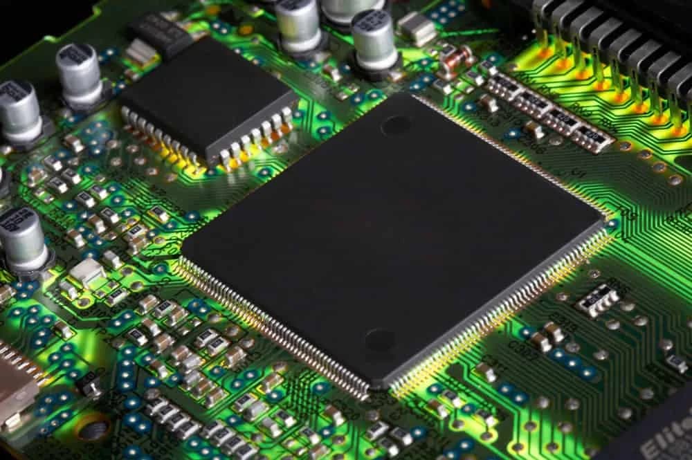
A via (Vertical Interconnect Access) is a plated hole that creates an electrical connection between two or more copper layers in a multilayer PCB. Every via consists of three parts: the barrel (plated hole wall), the pad (copper ring on each connected layer), and the antipad (clearance hole in non-connected planes).
The IPC-T-50 standard defines via terminology used across the industry. Via selection affects routing density, signal integrity, thermal performance, and manufacturing cost.
Through-Hole Vias (PTH)
Through-hole vias, also called plated through-holes, span the entire board thickness from top layer to bottom layer. A mechanical drill bit (typically 0.2mm to 0.5mm diameter) creates the hole, and electroplating deposits copper on the barrel wall.
When through-hole vias work best:
- Standard 2-layer and 4-layer boards where routing density isn't critical
- Power delivery paths that benefit from the full-stack copper connection
- Designs where cost matters more than board real estate
- Test point locations that need probe access from either side
Through-hole vias are the default choice for most PCB designs. Every fabricator handles them, lead times stay short, and yields remain high. The trade-off: they consume space on every layer, even layers that don't need the connection. On a 10-layer board, a through-hole via connecting only layers 1 and 4 still blocks routing on layers 2, 3, and 5 through 10.
Typical specifications:
| Parameter | Standard | High-Density |
|---|---|---|
| Drill diameter | 0.3-0.5mm | 0.2-0.25mm |
| Pad diameter | 0.6-0.9mm | 0.45-0.55mm |
| Aspect ratio | 6:1 | 8:1 max |
| Min. annular ring | 0.125mm | 0.075mm |
| Cost impact | Baseline | Baseline |
For basic designs, use the YourPCB Via Current Calculator to verify your via can handle the required current without overheating.
Blind Vias
Blind vias connect an outer layer (top or bottom) to one or more inner layers without passing through the entire board. The name comes from the fact that you can see the via from one side of the PCB but not the other.
Two drilling methods exist:
- Mechanical drilling before lamination: The fabricator drills partial-depth holes into a sub-laminate, plates them, then laminates the full stackup. Suitable for vias spanning 2-3 layers.
- Laser drilling after lamination: A UV or CO2 laser ablates through the outer copper and dielectric to reach the target inner layer. IPC defines laser-drilled blind vias with a diameter of 150 microns (6 mil) or less as microvias.
When blind vias make sense:
- BGA fan-out routing where through-hole vias won't fit between pads
- 6+ layer boards where you need routing channels on inner layers
- RF designs where stub elimination matters (a through-hole via on a 2.4GHz signal creates a stub that reflects energy back into the trace)
- Size-constrained designs like wearables or medical implants
Blind vias require sequential lamination. The fabricator builds the inner sub-laminate first, drills and plates the blind vias, then laminates the remaining layers. This adds 1-2 extra lamination cycles, increasing cost by 20-40% over a standard through-hole-only board.
Buried Vias
Buried vias connect two or more inner layers and never touch an outer surface. They are invisible from both sides of the finished PCB.
How they're manufactured:
The fabricator drills and plates buried vias on an inner sub-laminate before bonding it with the outer layers. For example, on an 8-layer board, a buried via might connect layers 3 and 6. The fabricator builds a 4-layer sub-laminate (layers 3-6), drills the buried vias, then laminates the outer layer pairs (1-2 and 7-8) on each side.
When buried vias pay off:
- Extremely dense designs where every routing channel counts
- High-layer-count boards (12+ layers) with complex internal signal routing
- Designs combining high-speed digital, analog, and power sections that need isolated internal routing
- Military and aerospace boards meeting IPC-6012 Class 3 reliability standards
Buried vias are the most expensive via type because they require the most complex fabrication sequence. Each buried via layer pair needs its own drill-and-plate cycle before lamination. Budget 40-80% cost premium over baseline through-hole designs.
A practical guideline: If your design can route with through-hole and blind vias alone, skip buried vias. They exist for boards where no other option works.
Microvias
Microvias are laser-drilled blind vias with a diameter of 150 microns (6 mil) or less and a maximum aspect ratio of 1:1, as defined by IPC-T-50. They connect adjacent layer pairs and are the foundation of HDI (High Density Interconnect) PCB technology.
What makes microvias different from standard blind vias:
- Drilled with UV or CO2 lasers, not mechanical bits
- Maximum diameter of 150 microns vs. 200+ microns for standard blind vias
- Span only one dielectric layer (adjacent layer pairs)
- Can be stacked or staggered to reach deeper layers
| Microvia Type | Description | Cost | Reliability |
|---|---|---|---|
| Single-level | Connects layer 1 to layer 2 only | Moderate | Excellent |
| Stacked | Multiple microvias aligned vertically (L1-L2-L3) | High | Good (requires copper filling) |
| Staggered | Microvias offset between layer pairs | Moderate-High | Excellent |
| Via-in-pad | Microvia placed directly under component pad, filled and capped | High | Excellent |
Stacked vs. staggered microvias: Stacked microvias save more space but require each level to be copper-filled before the next is drilled. IPC-2226 recommends limiting stacked microvias to 2-3 levels. Staggered microvias offset each level laterally, improving reliability at the cost of some routing space.
HDI boards with microvias enable routing densities 2-3x higher than conventional through-hole designs. This is how smartphone manufacturers fit 10+ billion transistors worth of connectivity into a board smaller than a credit card.
Via-in-Pad Design
Via-in-pad (VIP) places a via directly inside a component's solder pad rather than routing a trace to a nearby via. The technique eliminates the trace-to-via dog-bone pattern, saving critical space under fine-pitch components.
The process requires three steps:
- Drill and plate the via (typically a microvia or small through-hole)
- Fill the via barrel with conductive or non-conductive epoxy
- Cap and planarize the filled via so the pad surface is flat for soldering
Without filling, solder wicks down the via barrel during reflow, creating voids that weaken the joint. IPC-4761 Type VII defines the filled-and-capped via-in-pad standard.
Via-in-pad is essential for:
"For teams designing 6-layer and 8-layer boards, library control and DRC rule coverage matter more than UI polish, because one missed clearance rule can burn a full prototype spin."
Hommer Zhao, Founder & CEO, WIRINGO
- BGAs with pitch below 0.8mm (the dog-bone pattern won't fit between pads)
- QFN and DFN packages that need thermal vias directly under the exposed pad
- High-speed designs where the trace stub from a dog-bone adds unwanted inductance
Tented and Plugged Vias
Not every via needs to be exposed. Tenting and plugging protect vias from environmental contamination and prevent solder bridging during assembly.
Tented vias are covered with solder mask. This is the most common and cheapest protection method. The mask film bridges across the via opening, but it can crack on vias larger than 0.3mm diameter.
Plugged vias are filled with non-conductive epoxy, then covered with solder mask. More reliable than tenting for larger vias. Prevents outgassing during reflow that can cause solder defects on nearby pads.
Epoxy-filled and capped vias (IPC-4761 Type VII) are fully filled, planarized, and re-plated. Required for via-in-pad applications.
Backdrilled Vias
Backdrilling removes the unused portion of a through-hole via's barrel to eliminate signal stubs. A controlled-depth drill bit, slightly larger than the original hole, removes the unwanted copper plating.
This technique matters for signals above 3 GHz. At those frequencies, a 1mm stub on a through-hole via creates a resonant antenna that reflects signal energy. The reflection shows up as insertion loss and return loss degradation in S-parameter measurements.
When to backdrill:
- PCIe Gen 4/5, 10G+ Ethernet, or DDR5 interfaces
- Any differential pair running above 5 Gbps
- Through-hole vias on boards thicker than 2mm where the stub exceeds 10% of the signal wavelength
Backdrilling adds cost (typically $0.01-0.03 per hole), but it's far cheaper than switching to a full blind-via stackup when you only need stub removal on a few critical nets.
Cost Comparison
The via type you choose has a direct impact on fabrication cost. Here's a realistic comparison for a 6-layer, 1.6mm board:
| Via Type | Relative Cost | Lead Time Impact | Min. Fab Capability |
|---|---|---|---|
| Through-hole only | 1x (baseline) | Standard | Any fabricator |
| + Blind vias | 1.3-1.5x | +2-3 days | Mid-tier fab |
| + Buried vias | 1.5-1.8x | +3-5 days | Advanced fab |
| + Microvias (1 level) | 1.4-1.6x | +2-4 days | HDI-capable fab |
| + Stacked microvias | 2.0-3.0x | +5-7 days | Specialized HDI fab |
| + Backdrilling | 1.05-1.1x | +1 day | Most fabs |
The cost multipliers above are per-panel estimates. Actual pricing depends on layer count, board size, quantity, and the specific fabricator. Always request quotes with and without advanced via types so you can make data-driven decisions.
Design Rules and Best Practices
Aspect ratio is the single most critical via design rule. It's the ratio of board thickness to drilled hole diameter. Higher aspect ratios make reliable plating harder because the electroplating solution can't reach deep into narrow holes evenly.
| Via Type | Max Aspect Ratio | Reason |
|---|---|---|
| Through-hole | 10:1 (standard), 12:1 (advanced) | Plating uniformity degrades in deep, narrow holes |
| Blind via | 1:1 (laser), 8:1 (mechanical) | Laser drills have limited depth; mechanical drills need clearance |
| Microvia | 0.75:1 to 1:1 | IPC-2226 recommendation for reliable copper fill |
| Buried via | 8:1 | Same mechanical plating constraints as through-hole |
Annular ring is the copper pad width around the drilled hole. IPC-6012 Class 2 requires a minimum 50-micron annular ring; Class 3 requires 75 microns. Drill wander during fabrication can shift the hole off-center, so design your pads with margin.
Thermal relief patterns connect via pads to copper planes through narrow spokes instead of a solid connection. Without thermal relief, large plane connections act as heat sinks that make soldering difficult. Use 4-spoke thermal relief with 0.2-0.3mm spoke width for standard vias.
For impedance-controlled designs, via transitions create discontinuities. Use the YourPCB Impedance Calculator to model the impact of vias on your controlled-impedance traces.
Choosing the Right Via Type for Your Design
Start with through-hole vias. Only add complexity when the design demands it. Here's a decision framework:
- Can you route everything with through-hole vias? If yes, stop. You're done.
- Do you have fine-pitch BGAs (< 0.8mm pitch)? Use blind microvias or via-in-pad for fan-out.
- Are inner-layer routing channels blocked by through-hole via barrels? Consider blind vias to free up specific layers.
- Do you have high-speed signals (> 5 Gbps) through thick boards? Use backdrilling or blind vias to eliminate stubs.
- Is the board so dense that blind vias alone can't route it? Add buried vias as a last resort.
This hierarchy keeps costs down while solving real routing problems. Over-specifying via types is one of the most common PCB cost traps. A 4-layer board rarely needs blind vias. A 6-layer board almost never needs buried vias.
References
- IPC-T-50: Terms and Definitions for Interconnecting and Packaging Electronic Circuits
- IPC-2226: Sectional Design Standard for HDI Printed Boards
- Scattering Parameters (S-Parameters) - Signal Integrity
- PCB Via Design Guide - Sierra Circuits
- Blind, Buried & Micro Via Definition - Altium Documentation
Frequently Asked Questions
What's the difference between a blind via and a buried via?
A blind via connects an outer layer to an inner layer and is visible from one side of the board. A buried via connects only inner layers and is hidden from both surfaces. Both require sequential lamination during fabrication, but buried vias are more expensive because they need separate drill-and-plate cycles on inner sub-laminates before the full board is assembled.
I need to route a 0.5mm-pitch BGA. Should I use microvias or standard blind vias?
Microvias. At 0.5mm pitch, BGA pads are roughly 0.25mm in diameter with 0.25mm gaps between them. A standard mechanically-drilled blind via (minimum ~0.2mm drill) with its pad won't fit between adjacent pads. Laser-drilled microvias with 0.1mm drill and 0.25mm pad allow fan-out routing directly under the package using a via-in-pad approach.
Do blind and buried vias affect signal integrity?
Blind and buried vias generally improve signal integrity compared to through-hole vias for signals above 1 GHz. Through-hole vias on high-frequency signals create stubs: the unused barrel portion acts as an antenna that reflects energy. Blind vias eliminate the stub entirely. If your design uses through-hole vias on high-speed nets, consider backdrilling (cheaper) or blind vias (cleaner) to remove stub effects.
How much do microvias add to the cost of a PCB?
Single-level microvias (connecting adjacent layers) typically add 30-60% to fabrication cost compared to a through-hole-only board of the same layer count. Stacked microvias with copper filling can double or triple the cost. The actual premium depends on your fabricator's HDI capabilities: factories with dedicated laser-drill lines and sequential lamination presses absorb the cost better than general-purpose shops.
Can I mix via types on the same board?
Yes, and most complex designs do exactly this. A typical HDI smartphone board uses through-hole vias for power and ground connections, blind microvias for BGA fan-out on outer layers, buried vias for inner-layer signal routing, and backdrilled vias for high-speed serializer/deserializer (SerDes) interfaces. The key is to use the simplest via type that meets each specific routing need.
When should I use via-in-pad instead of a standard dog-bone fan-out?
Use via-in-pad when the component pitch is too tight for dog-bone routing (typically below 0.8mm BGA pitch), when thermal performance requires vias directly under an exposed pad (QFN/DFN packages), or when signal path length is critical and you can't afford the extra trace length of a dog-bone. Via-in-pad costs more due to the fill-and-cap process, so avoid it when dog-bone routing works fine.
"I look for three outputs before I trust any PCB CAD flow: netlist consistency, manufacturing outputs checked against IPC naming conventions, and a 3D review that catches connector interference before release."
Hommer Zhao, Founder & CEO, WIRINGO
If you want to turn this topic into a production decision, review our EDA comparison reference, check the supporting numbers on the EDA shortcuts reference, and use the contact page if you need a second review before release.


Need Help with Your PCB Design?
Check out our free calculators and tools for electronics engineers.
Browse PCB Tools"In over 20 years of manufacturing experience, we have learned that quality control at the component level determines 80% of field reliability. Every specification decision you make today affects warranty costs three years from now."
— Hommer Zhao, Founder & CEO, WIRINGO