
Backplane PCB manufacturing succeeds or fails on stackup control, connector strategy, press-fit discipline, impedance targets, and test access. This buyer-focused guide explains what to define before fabrication and assembly release.
For more information on industry standards, see printed circuit board and IPC standards.
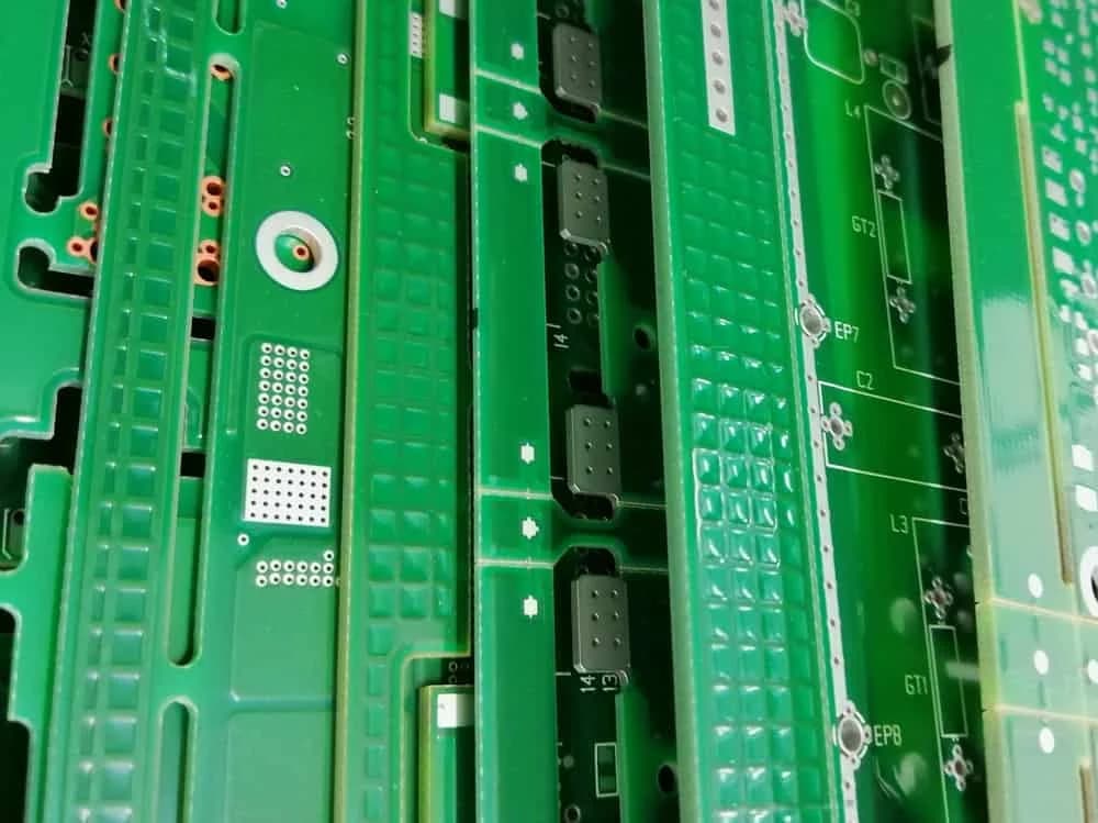
A backplane PCB looks simple from a distance: a large board, rows of connectors, power distribution, and high-speed channels between plug-in cards. In production, it is one of the easiest assemblies to underestimate. The board is often thick, the copper weight may be heavy, connectors are expensive, press-fit insertion force can damage barrels, and a small impedance error can affect every slot in the system.
A backplane is a structural and electrical backbone for a modular system. For background, see backplane, printed circuit board, signal integrity, and electrical connector. If you are sourcing a new program, pair this guide with our backplane PCB, high speed backplane connectors, impedance control PCB manufacturing, ICT testing service, and turnkey electronics manufacturing resources.
Why backplane PCB manufacturing is different
Backplanes concentrate risk. A daughtercard can usually be revised without changing the whole system architecture. A backplane mistake can affect every card, every connector, every power rail, and every enclosure fit. That is why buyers should treat the backplane as a controlled platform, not as a large version of a normal 4-layer board.
The first difference is mechanical. Backplanes are often thicker than common PCB assemblies, sometimes 2.4 mm, 3.2 mm, or more depending on connector retention, panel stiffness, and copper distribution. That thickness changes drilling, plating, lamination, depaneling, and inspection strategy. A high aspect-ratio via or connector barrel may need tighter process review than the buyer expects.
The second difference is electrical. Backplanes may carry multi-gigabit differential pairs, clock distribution, high-current power planes, management buses, and low-speed control signals in the same board. Stackup, material selection, via geometry, reference-plane continuity, and connector launch design have to be locked together.
A backplane is not just a routing board. It is the part that forces electrical, mechanical, connector, and test decisions to agree. If one discipline is released late, the whole system usually pays for it.
— Hommer Zhao, Technical Director
The third difference is assembly stress. Large connectors, guide hardware, press-fit pins, and through-hole features can create forces that a normal SMT-centered PCBA never sees. The assembly plan must protect plating, hole size, board flatness, and connector seating before production starts.
The buyer checklist before releasing Gerbers
Before a backplane goes to fabrication, the buyer should freeze more than the Gerber package. A usable release should define stackup, material family, copper weights, finished thickness tolerance, controlled impedance targets, connector part numbers, drill tolerances, press-fit hole requirements, final surface finish, test coupon rules, and acceptance criteria.
The most expensive errors usually happen when one of those items is implied instead of specified. For example, the connector datasheet may require a finished hole window that is narrower than the fabricator normally holds on a thick board. If the drawing only says plated through hole, the factory may build a board that passes generic inspection but fails connector insertion.
Backplane control table
| Control point | What to define | Typical number or rule | Who should approve it | Risk if missed |
|---|---|---|---|---|
| Finished thickness | Nominal thickness and tolerance | 2.4 mm, 3.2 mm, or project-specific stackup | Mechanical and PCB engineering | Connector fit, enclosure alignment, and bow problems |
| Controlled impedance | Single-ended and differential targets | 50 ohm single-ended or 85 to 100 ohm differential | Signal integrity owner | Reflections, eye margin loss, and slot-to-slot variation |
| Press-fit holes | Drill, plating, finished-hole window, and annular ring | Connector datasheet tolerance, often much tighter than generic PTH | Connector supplier and fabricator | Barrel cracking, low retention, or excessive insertion force |
| Copper balance | Plane distribution, heavy copper zones, thieving if needed | Review any 2 oz or 4 oz copper area against lamination plan | PCB fabricator | Warpage, resin starvation, and uneven plating |
| Connector seating | Coplanarity, keepouts, tooling holes, insertion support | Fixture support under connector rows | Assembly engineering | Tilted connectors and damaged board laminate |
| Test access | ICT, flying probe, boundary scan, or fixture test plan | Define pads, rails, nets, and records before layout freeze | Test engineering | Late fixture redesign and weak fault isolation |
| Documentation | Revision-controlled drawing notes and acceptance criteria | Match BOM, Gerbers, drill files, stackup, and assembly notes | Buyer quality team | Mixed revisions and supplier interpretation gaps |
Use the table as a release checklist, not as a generic preference list. Each row should have an owner and evidence before the purchase order is placed.
Stackup and impedance decisions
Backplane stackup is where many programs lose margin. The board may need enough layers for routing density, enough plane continuity for return currents, enough copper for power distribution, and enough dielectric control for impedance. Those needs can conflict. A thicker board may improve stiffness but make via stubs and drilling harder. A material change may help loss but change cost, lead time, and fabrication yield.
For lower-speed control backplanes, standard FR-4 may be sufficient. For high-speed serial links, buyers should ask for insertion-loss expectations, dielectric constant control, glass-weave risk, and coupon-based impedance verification. If the design uses 10 Gbps, 25 Gbps, or faster lanes, the supplier should not guess. The release should identify the target impedance, tolerance, reference layers, and whether backdrilling or blind/buried vias are required.
If the backplane has 100 ohm differential pairs but no controlled stackup drawing, the impedance target is only a wish. The fabricator needs dielectric thickness, copper weight, trace geometry, and test coupon rules before CAM work starts.
— Hommer Zhao, Technical Director
Buyers should also watch via stubs. A connector field can create long plated barrels, especially on thick boards. If high-speed channels pass through the full thickness but only use certain layers, unused via length can become a signal-integrity problem. Backdrilling, routing layer choice, and connector launch geometry should be discussed during DFM, not after first articles fail a link test.
Connector and press-fit requirements
Backplane connectors often decide the manufacturing plan. Press-fit connectors are attractive because they avoid soldering many high-pin-count connector rows, but they transfer large force into plated holes. The hole size, plating thickness, barrel quality, and insertion tooling must match the connector system.
A press-fit requirement should never be reduced to install connector after fabrication. The drawing should include the connector manufacturer, part number, finished-hole range, plating requirement, insertion direction, support fixture concept, inspection method, and rework rule. The assembly team also needs a way to confirm seating height and detect damaged barrels.
Soldered connectors create a different risk profile. They may require selective soldering, wave soldering, hand soldering, or custom fixtures depending on board size and thermal mass. Large ground pins and heavy copper planes can steal heat, while plastic connector bodies can limit process temperature. If solder fill must meet a specific workmanship class, define it before assembly.
For programs that combine backplanes with cable exits, front-panel connectors, or enclosure wiring, review the connector plan alongside electronic assembly services and box-level manufacturing expectations. A connector that passes on the bench can still fail when the enclosure forces misalignment or cable strain.
Power distribution and thermal margin
Backplanes often carry several power rails across multiple slots. The question is not only whether the copper can carry current. Buyers should also check voltage drop, connector pin current, hot-swap behavior, fuse strategy, plane neck-downs, and heat rise around high-current regions.
A common mistake is approving a beautiful signal-routing layout while leaving power integrity to generic plane shapes. A 20 A rail distributed across multiple cards needs more than a wide copper pour. It needs defined current paths, return paths, connector pin grouping, copper weight, thermal relief strategy, and test limits. If one slot can pull more current than the others, the board should be reviewed for worst-case loading, not average loading.
Thermal considerations also affect assembly. Thick copper and large planes can make soldering difficult, especially around power connectors or bus bars. The factory may need selective solder profiles, preheat control, or fixture support to achieve repeatable solder fill without damaging neighboring parts.
Test strategy for backplane production
A backplane test plan should be written before layout freeze because many defects are easier to prevent than diagnose. Electrical continuity alone is usually too weak for a serious system backplane. Buyers should consider netlist electrical test for the bare board, impedance coupons, ICT or flying probe for assembled boards, connector seating inspection, hipot or insulation checks where needed, and functional slot-to-slot verification.
For dense connector fields, ICT access may be limited, but that does not remove the need for fault isolation. Boundary scan, loopback cards, golden daughtercards, or fixture harnesses can help prove paths between slots. The test should produce records that identify the failed net, slot, connector, rail, or lane rather than only saying pass or fail.
The best backplane test plan tells the repair team where to look. A fail code that names slot 4, connector J12, differential pair TX3, or a 12 V rail saves far more time than a generic system failed message.
— Hommer Zhao, Technical Director
Backplane inspection should also include mechanical checks. Connector height, perpendicularity, insertion damage, board bow, and hardware torque can matter as much as electrical continuity. If the board plugs into an enclosure card cage, first-article inspection should include physical mating with real or representative cards.
Common sourcing mistakes
The first mistake is asking for a quote before the connector and stackup are stable. Suppliers can price the board, but the number may be meaningless if the final design later adds press-fit connectors, tighter impedance, backdrilling, or thicker copper.
The second mistake is treating press-fit holes as normal plated holes. Press-fit technology lives inside a narrow process window. A hole that is slightly oversized can lose retention, while a hole that is slightly undersized can crack plating during insertion.
The third mistake is separating mechanical and electrical reviews. Slot pitch, board thickness, guide hardware, connector retention, trace routing, and power planes all interact. A backplane DFM review should include mechanical drawings and mating hardware, not only PCB files.
The fourth mistake is leaving test ownership undefined. Bare-board electrical test, impedance coupons, assembled-board inspection, and final system verification each catch different risks. If the buyer does not assign the risks clearly, every supplier assumes a narrower responsibility than the system needs.
Practical RFQ language buyers can use
A strong RFQ can be concise. It should say that the supplier must review the released stackup for controlled impedance, confirm press-fit hole capability against the named connector datasheet, identify any high-aspect-ratio drilling concerns, propose bare-board and assembled-board test coverage, and flag connector insertion tooling before fabrication starts.
Also ask for the supplier to return exceptions in writing. Silence should not mean approval. For a backplane, the most useful supplier response is often an exception list: hole tolerance risk, connector availability, preferred surface finish, backdrill recommendation, panelization limit, or fixture requirement.
For first articles, require actual records: impedance coupon readings, bare-board test status, connector seating measurements, inspection photos if needed, and functional or continuity logs by serial number. Those records are what let the team move from sample approval to repeat production without rediscovering the same questions.
FAQ
Q: What makes backplane PCB manufacturing harder than standard PCB fabrication?
Backplanes often combine thick boards, high connector density, controlled impedance, heavy copper, and tight mechanical fit. A 3.2 mm board with press-fit connectors and 100 ohm differential pairs has fabrication and assembly risks that a simple 1.6 mm FR-4 control board does not have.
Q: Should a backplane use press-fit or soldered connectors?
It depends on pin count, serviceability, connector system, board thickness, and process capability. Press-fit avoids soldering many pins but requires a controlled finished-hole window and insertion tooling. Soldered connectors may be better for some lower-density designs but can need selective solder profiles and strong thermal control.
Q: What impedance should I specify for high-speed backplane traces?
Many systems use 85 ohm or 100 ohm differential impedance, while some single-ended nets use 50 ohm. The exact value must match the interface standard and connector launch. The RFQ should include target impedance, tolerance, layer reference, and coupon test requirements.
Q: Is bare-board electrical test enough for a backplane PCB?
No for most assembled backplanes. Bare-board test catches opens and shorts before assembly, but it does not prove connector seating, press-fit barrel health after insertion, solder quality, slot-to-slot behavior, or final mechanical fit. Add assembled-board inspection or functional slot testing where the system risk requires it.
Q: When should backdrilling be considered on a backplane?
Backdrilling should be reviewed when thick-board via stubs affect high-speed channels. If the backplane routes multi-gigabit lanes through a 2.4 mm or 3.2 mm board, unused plated barrel length can reduce eye margin, so signal-integrity review should happen before layout release.
Q: What documents should buyers send with a backplane RFQ?
Send Gerbers, drill files, IPC netlist if available, stackup drawing, controlled impedance table, connector datasheets, assembly drawing, mechanical envelope, test requirements, and expected annual volume. The supplier needs all of these to price tooling, drilling, insertion, inspection, and test correctly.
Final takeaway
Backplane PCB manufacturing is successful when the buyer locks the decisions that connect fabrication, assembly, connectors, mechanics, signal integrity, and test. The supplier can build the board only as well as the release package defines those decisions. Stackup, impedance, press-fit holes, connector seating, power distribution, and test records should all be explicit before first articles.
If you need help reviewing a backplane stackup, connector plan, press-fit requirement, or production test strategy, contact our team. We can support the transition from concept layout to manufacturable backplane assembly with the right controls defined before release.
Related Articles
High-Volume PCB Manufacturing RFQ: What Buyers Must Freeze Before 600,000 Units per Year

Box Build Assembly Checklist: What OEM Buyers Should Freeze Before Pilot Production

Selective Soldering in PCB Assembly: When Buyers Should Specify It and What Must Be Locked Before Release
Need Help with Your PCB Design?
Check out our free calculators and tools for electronics engineers.
Browse PCB Tools"In over 20 years of manufacturing experience, we have learned that quality control at the component level determines 80% of field reliability. Every specification decision you make today affects warranty costs three years from now."
— Hommer Zhao, Founder & CEO, YourPCB