Through-hole soldering with process evidence
Wave Soldering PCB Assembly for Through-Hole Lots That Need Stable Release
YourPCB supports wave soldering PCB assembly when high-pin-count through-hole boards need faster, more repeatable soldering than manual work, with DFM review for pallets, preheat risk, IPC-A-610 inspection, and release records before shipment.

TL;DR
- Wave soldering fits pure THT and simple mixed boards with a clear bottom-side solder path.
- Selective soldering is safer when bottom-side SMT or heat-sensitive parts sit near the joints.
- RFQs should include Gerbers, BOM, XY data, assembly drawings, alloy, class, and test needs.
- Release control should cover flux, preheat, first article, inspection, touch-up, and exceptions.
What This Service Covers
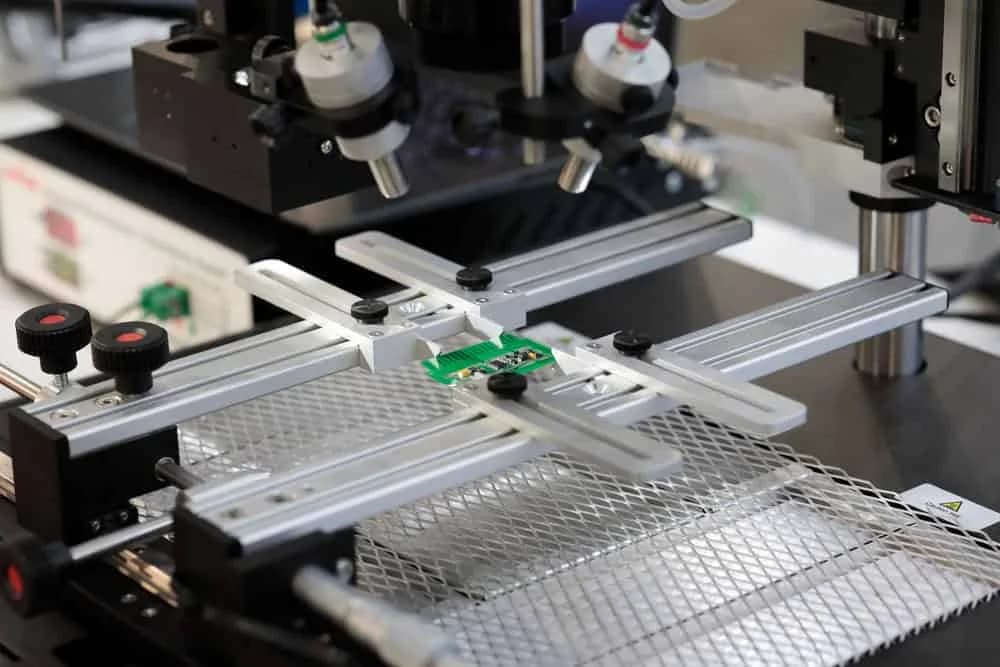
Wave soldering PCB assembly is a factory process for soldering many through-hole joints as a board passes over a controlled solder wave. A wave pallet is a protective carrier that exposes only the solderable areas of a mixed-technology PCBA. A release record is the lot-level evidence that ties the solder route, inspection status, exceptions, and shipment decision to the approved build revision.
This service differs from through-hole PCB assembly because it focuses on the wave soldering route itself: flux, preheat, conveyor exposure, pallet risk, touch-up limits, and release evidence. It also differs from selective soldering, which solders localized joints when the full bottom side cannot safely see the wave.
Standards give the buyer and factory a shared reference. IPC electronics standards provide context for IPC-A-610 solder-joint acceptability and IPC-J-STD-001 soldered assembly process control. ISO 9000 quality management explains why revision control, nonconforming output handling, and release records matter when a PCBA repeats across multiple lots.
Wave Soldering Capabilities
Wave-Ready DFM Review
Gerbers, ODB++, BOM, XY data, and assembly drawings are checked for bottom-side exposure, component height, lead protrusion, thermal relief, and pallet needs before quoting.
Flux and Preheat Planning
Flux type, spray coverage, preheat ramp, board thickness, copper weight, and heat-sensitive bodies are reviewed so lead-free SAC305 soldering does not create cold joints or scorched parts.
Through-Hole Solder Coverage
Headers, connectors, transformers, relays, terminal blocks, switches, LEDs, and radial or axial components can be wave soldered when the layout allows stable wave contact.
Mixed-Technology Pallet Review
Simple mixed SMT/THT boards are reviewed for wave pallets, solder dams, keep-outs, and bottom-side component protection before we recommend wave soldering over selective soldering.
IPC-A-610 Inspection Focus
Through-hole joints are checked for barrel fill, wetting, bridging, icicles, solder balls, residue, lead protrusion, connector seating, and polarity against the agreed class target.
Lot Release Records
First-article notes, process route, solder alloy, inspection status, rework holds, and shipment exceptions are kept visible for prototype, pilot, and repeat production lots.
Capability Table
| Best-fit boards | Pure through-hole PCBAs and simple mixed SMT/THT boards with a clear bottom-side solder path |
|---|---|
| Companion processes | SMT reflow, manual insertion, wave soldering, touch-up, cleaning review, AOI, visual inspection, and functional test handoff |
| Solder alloy planning | Lead-free SAC305 for RoHS programs; leaded processing only when the product scope allows it |
| Quote inputs | Gerber or ODB++, BOM, XY data, assembly drawing, revision notes, quantity breaks, solder alloy, and inspection class |
| Inspection reference | IPC-A-610 acceptability context plus buyer-specific connector seating, polarity, and test notes |
| Common risk points | Bottom-side SMT exposure, tall plastic bodies, heavy copper thermal sinks, insufficient annular ring, and uncontrolled lead protrusion |
| Best volume fit | Prototype validation, pilot lots, bridge builds, low-volume production, and repeat batches where setup consistency matters |
| Out of scope | Boards with dense bottom-side SMT under the wave path, undefined orientation, no release criteria, or components that cannot tolerate soldering heat |
Wave, Selective, or Hand Soldering?
The lowest-risk soldering route depends on bottom-side exposure, joint count, component heat tolerance, and whether the build is a stable repeat lot or a changing prototype. A wave process can be efficient, but a poor wave candidate can cost more after touch-up, rework, and schedule slips.
| Buyer situation | Best-fit route | Why it matters |
|---|---|---|
| Pure through-hole board with many connectors | Wave soldering | The solder wave reaches many joints in one pass, so the buyer gets lower handling variation than manual soldering. |
| Mixed board with no bottom-side SMT in the solder path | Wave soldering with pallet review | A pallet can protect areas that should not see the wave while keeping high-pin-count connectors efficient. |
| Mixed board with bottom-side SMT near through-hole pins | Selective soldering | A programmable nozzle avoids full-wave exposure and usually reduces damage risk around dense surface-mount parts. |
| Prototype with 5 boards and unstable layout | Controlled hand soldering | Early engineering lots may not justify pallet or process setup until connector locations and test limits stabilize. |
The decision is not only process speed. A 5-board prototype with unstable drawings may be better as controlled hand soldering, while a 500-board repeat lot with many connectors may justify wave setup or pallet work. YourPCB flags that boundary before the buyer spends tooling money in the wrong place.
Wave Soldering Workflow
1
RFQ and Board Fit Review
We review the PCB files, BOM, quantities, solder alloy, bottom-side layout, component height, and inspection target to decide whether wave soldering is the right process.
2
DFM and Pallet Decision
Engineering checks wave access, solder-mask dams, thermal relief, keep-outs, lead length, and whether a wave pallet is needed for simple mixed-technology assemblies.
3
SMT, Insertion, and Preheat Setup
If the board has SMT parts, reflow happens first. Through-hole parts are then inserted, checked for polarity and seating, and prepared for flux and preheat.
4
Wave Soldering and Touch-Up Control
The lot runs through the wave process with controlled flux, preheat, conveyor direction, and solder alloy. Touch-up is limited and recorded when required.
5
Inspection and Release
Through-hole joints are inspected for wetting, fill, bridges, icicles, residue, and connector seating before the PCBA moves to testing, coating, box build, or shipment.
Capability Scope and Buyer Limits
Wave soldering works best when the board design gives the solder wave a clean path. YourPCB reviews pure through-hole PCBAs, connector-heavy boards, power boards, and simple mixed boards where a pallet can protect selected areas. The RFQ should state the solder alloy, inspection class, cleaning restrictions, functional test needs, and whether the PCBA will later move into harness mating, coating, or enclosure assembly.
The service is not the right fit for every mixed-technology board. Dense bottom-side SMT, heat-sensitive plastic bodies, undefined component orientation, unstable lead length, or missing pass/fail criteria can move the recommendation toward selective soldering or controlled hand soldering. That limitation is intentional: selecting the wrong solder route usually costs more than using the slower process from the start.
An Australia automotive-electronics program from 2025-Q2 to 2025-Q3 expanded from harness work into PCBA through "cross-category expansion" and "multi-department client engagement". In wave soldering terms, that means the buyer should not isolate soldering from connector, harness, and final integration decisions. The through-hole joint may be strong, but the program still fails if the mating interface is released late.
Author and Quality Basis
This service page is written from YourPCB factory-side experience supporting PCB fabrication, SMT assembly, through-hole assembly, wire harness, cable assembly, electronic assembly, and box build programs for OEM buyers. Hommer Zhao reviews service content around the practical RFQ questions engineers and procurement teams ask before releasing prototype, pilot, and low-volume electronics builds.
The quality basis for this page is IPC-A-610 solder-joint acceptability context, IPC-J-STD-001 soldering process logic, ISO 9001-style record control, release-file discipline, and buyer-approved inspection and test limits.
Frequently Asked Questions
What is wave soldering PCB assembly?
Wave soldering PCB assembly is a through-hole soldering process where the bottom side of a loaded PCB passes over a controlled solder wave. It fits boards with many through-hole leads, connectors, relays, terminal blocks, or simple mixed SMT/THT layouts. For lead-free RoHS programs, SAC305 alloy and preheat control need to be reviewed before the run. The inspection plan should name IPC-A-610 class expectations and any buyer-specific connector seating or polarity checks.
When should I choose wave soldering instead of selective soldering?
Choose wave soldering when the board is mostly through-hole, the bottom side has no vulnerable SMT parts in the wave path, and many joints can be soldered in one pass. Choose selective soldering when bottom-side SMT, plastic bodies, keep-outs, or localized connectors make full-wave exposure risky. For a 100-board pilot lot, YourPCB normally reviews wave, selective, and controlled hand soldering before recommending the route because fixture cost, defect risk, and schedule are not the same.
What files do you need to quote wave soldering PCB assembly?
Send Gerber or ODB++ data, BOM, XY placement data, assembly drawings, component polarity notes, revision status, quantity breaks, solder alloy requirements, and test or inspection requirements. Wave soldering quotes need more than the bare board files because lead length, bottom-side keep-outs, component height, and pallet requirements affect the process. If IPC-A-610 Class 2 or Class 3 acceptance is required, state that target in the RFQ package before pricing.
I have 250 mixed SMT/THT boards. Is wave soldering still practical?
Wave soldering can be practical for 250 mixed SMT/THT boards when bottom-side SMT exposure is limited and the through-hole joints are numerous enough to justify setup or a pallet. If connectors sit near heat-sensitive packages or dense bottom-side parts, selective soldering may be safer even if the cycle time is slower. YourPCB reviews the XY file and bottom layer first, then flags whether wave soldering, selective soldering, or hand soldering gives the lowest total risk.
How do you control quality on lead-free wave soldered PCBAs?
Lead-free wave soldered PCBAs are controlled through flux coverage, preheat profile review, solder alloy control, conveyor setup, first-article inspection, and post-solder visual checks. IPC-A-610 provides the acceptability context for through-hole wetting, fill, bridging, icicles, and residue, while ISO 9000 quality management explains why revision and release records matter in repeat lots. Buyer-defined functional test limits should be added when visual inspection alone cannot prove the board works.
Can wave soldering be part of a turnkey electronics build?
Yes, wave soldering can sit inside a turnkey electronics build that includes PCB fabrication, component sourcing, SMT reflow, through-hole insertion, inspection, functional testing, cable mating, conformal coating, or box build assembly. The key is sequencing. Soldering and cleaning decisions should be locked before coating, and connector test access should be checked before enclosure work. For programs with PCBAs and harnesses, one release plan reduces unclear responsibility between suppliers.
Related Services
Through-Hole PCB Assembly
Use this page for the broader THT scope covering component selection, insertion, wave, selective, hand soldering, and inspection choices.
Selective Soldering PCB Assembly
Use selective soldering when bottom-side SMT parts, keep-outs, or localized connectors make full wave exposure too risky.
SMT PCB Assembly
Use SMT assembly when the primary build risk is solder paste, reflow, fine-pitch placement, AOI, or X-ray verification.
Box Build Assembly
Use box build when wave soldered PCBAs must be integrated with wiring, enclosure hardware, labeling, firmware, and final test.
Need a Wave Soldering Route Checked Before RFQ?
Send the Gerbers, BOM, XY file, assembly drawing, solder alloy, quantity, and inspection target. We will review whether wave, selective, or controlled hand soldering is the right release path.
Contact YourPCB