PCB Stencil Service
A good PCB stencil service does more than cut metal from a paste Gerber. It helps the SMT build print the right amount of solder paste, in the right places, with enough repeatability that the stencil does not become the hidden cause of bridging, opens, or unstable prototype results.
What This Service Actually Covers
Buyers looking for a PCB stencil service usually have one of two problems. Either they need a stencil quickly for a prototype SMT build, or they already know the board contains enough print-risk features that a generic default stencil could damage yield. In both cases, the real job is not only to cut apertures. It is to align stencil thickness, aperture geometry, and print strategy with the assembly process that will use the foil.
On this site, the nearest related pages are SMT PCB assembly, PCB assembly prototype, and instant PCB quote, and castellated hole PCB modules. This page sits one level lower in the process. It focuses on the stencil as a buying-intent service for boards that will move into solder paste printing, pick-and-place, and reflow without leaving paste volume to guesswork.
Why Stencil Decisions Matter More Than Many Buyers Expect
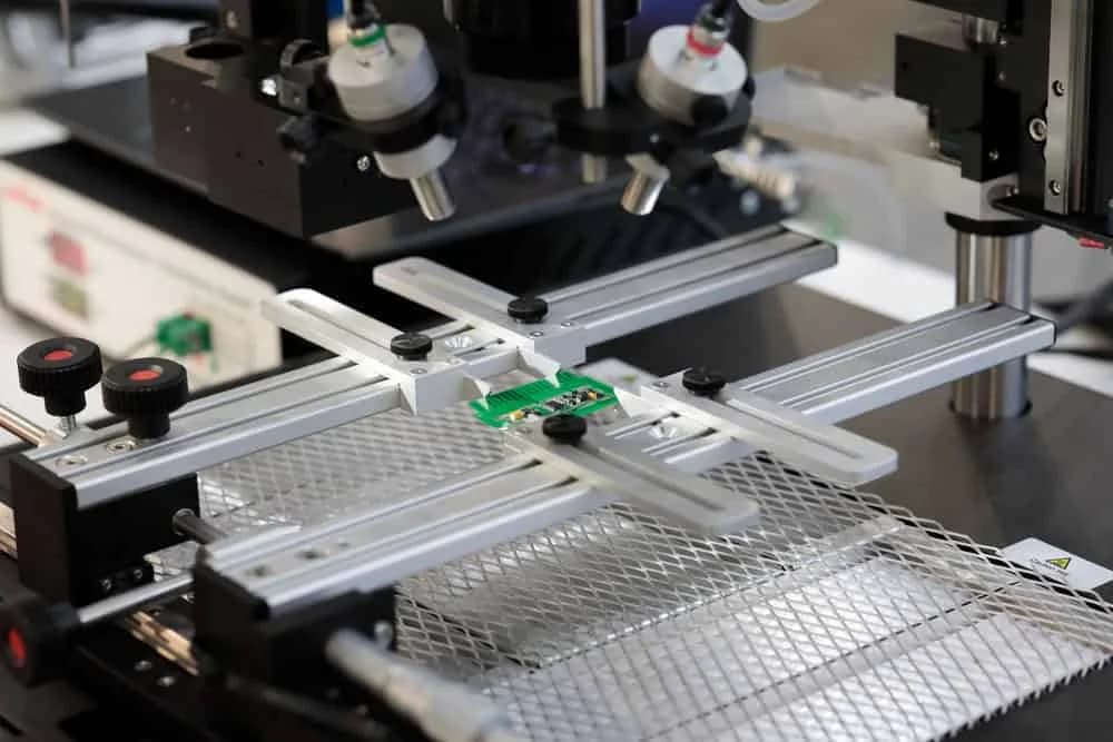
Laser-Cut Stainless Steel
Stencil supply is built around laser-cut stainless steel for consistent aperture definition, smoother paste release.
Assembly-Aware Aperture Review
We review the stencil against the assembly intent, including fine-pitch packages, thermal pads, bottom-terminated devices.
Prototype to Production Fit
The same page supports prototype stencil sourcing, engineering validation runs, and production handoff where frame style, panel strategy.
Linked to Real SMT Process
Stencil planning is tied to paste printing, placement, reflow, AOI, and rework risk rather than treated as a disconnected procurement line item.
Useful for Standalone Supply or Full Build
Customers can order a stencil only, or align it with PCB fabrication, SMT assembly, through-hole operations, cable integration, or box-build support.
Design Risk Surfaced Early
Fine apertures, area-ratio issues, large exposed pads.
Where a Stencil Usually Goes Wrong
The common failure is assuming the solder paste output from CAD should be cut directly without process judgment. That works only when the board is very forgiving. Once the assembly includes bottom-terminated packages, fine-pitch pads, large thermal pads, or panel constraints, the stencil becomes a process-control tool, not a commodity sheet.
A proper stencil review looks at solder paste transfer efficiency, aperture area ratio, thermal-pad windowing, and whether the print method is manual, semi-automatic, or inline. Those factors drive whether the first print is stable or whether the team spends the build cleaning bridges and chasing insufficient solder defects.
For background on the process itself, it helps to understand solder paste behavior and the role of a stencil in repeatable printing. Material choice also matters, which is why most SMT programs rely on stainless steel foils for dimensional stability and durability.
Service Specifications
| Typical material | Laser-cut stainless steel stencil foils selected for SMT paste printing repeatability |
|---|---|
| Common use cases | Prototype PCBA, NPI builds, low-volume SMT, pilot production, and repeat assembly programs |
| Review focus | Aperture geometry, stencil thickness, thermal-pad windowing, fine-pitch paste transfer, panel alignment, and printer fit |
| Input package | Paste Gerber layers, board outline, panelization notes, side identification, and assembly files when stencil planning is tied to PCBA |
| Output options | Prototype stencil supply, framed or frameless planning, and stencil guidance linked to assembly workflow |
| Typical adjacent services | SMT PCB assembly, prototype assembly, instant quote review, and full fabrication-to-assembly handoff |
How The Stencil Workflow Fits The Build
1
Review paste data and package mix
We start with the paste layers, outline, and package mix because stencil decisions depend on the real smallest apertures, largest pads.
2
Adjust stencil strategy to the print process
Prototype hand printing, semi-automatic printing, and full inline SMT printing do not use the same process window. We align thickness, foil style.
3
Check aperture risk before cutting
Fine-pitch pads, area-ratio limits, exposed thermal pads.
4
Release the stencil with assembly context
If the stencil is part of a full PCB assembly program, we keep the stencil aligned with placement, reflow, AOI.
5
Support repeat builds and revisions
When designs evolve, stencil revisions are managed with the same practical focus as the board revision so the next print run does not inherit outdated aperture data.
Fine-Pitch SMT Programs
QFN, BGA, and bottom-terminated components need stencil decisions that protect paste release and reduce the chance of bridging, opens, and voiding.
Prototype and NPI Builds
Engineering teams usually need quick-turn stencil support that still reflects real printability, not just a file conversion from CAD output to metal.
Mixed-Technology Assemblies
Boards with both delicate SMT features and large thermal or connector pads benefit from aperture balancing before the first run moves into production.
Files That Help Us Quote The Stencil Correctly
- Paste Gerber data for each assembled side
- Board outline and panelization details if the job is arrayed
- Part mix with any fine-pitch, BGA, or bottom-terminated packages called out
- Known stencil preferences such as thickness, frame style, or printer format
- Assembly files if the stencil will be used for a full SMT or turnkey build
- Revision control so stencil and PCB data stay aligned across reruns
If the board is also moving into fabrication or assembly, combine the stencil request with the full build package through our instant PCB quote workflow. That reduces the chance of quoting the stencil against outdated paste data or the wrong panel assumptions.
Frequently Asked Questions
What files do you need to make a PCB stencil?
The fastest package includes Gerber data for the paste layers, board outline, panelization notes if the build is arrayed, component side identification, and any known aperture adjustments for fine-pitch or thermal-pad areas. If assembly is planned at the same time, the BOM and placement data help us review stencil needs against the real build instead of only the paste Gerber.
What stencil thickness should I choose for SMT assembly?
Stencil thickness depends on the smallest aperture, the largest thermal pad, and the real mix of package types on the board. Many prototype and low-volume SMT jobs land around 0.10 mm to 0.15 mm stainless steel, but that is not a universal rule. Fine-pitch QFN, 0.4 mm to 0.5 mm pitch BGA, and large power pads often need aperture tuning instead of a generic thickness choice.
Can one stencil work for both prototype and production?
Sometimes, but only if the paste transfer requirements, panel setup, and print process stay close enough. A prototype stencil may be optimized for manual printing or quick engineering changes, while a production stencil may need stronger frame strategy, repeatability on automated printers, and more conservative aperture modifications for yield.
Do you review aperture reductions and home-plate shapes?
Yes. A stencil service is more useful when it reviews the buyer's real assembly risk. That includes fine-pitch apertures, area-ratio risk, thermal-pad windowing, home-plate changes for passive parts where tombstoning is a concern, and paste volume control around large connectors or mixed-technology boards.
Is this only for stencil supply or for full PCB assembly too?
It can be either. Some customers only need a laser-cut stencil. Others need the stencil aligned with SMT PCB assembly, prototype runs, or a full turnkey build. The important point is that stencil design should match the assembly intent, not sit as an isolated purchasing item.
When should I order a framed stencil instead of a prototype stencil?
Choose a framed stencil when the board will run on a dedicated printer, the volume justifies better print repeatability, or the process window is tight enough that fixture stability matters. Prototype and low-volume jobs often use frameless foils or quick-turn options, but production printing usually benefits from a frame strategy matched to the machine and board size.
Need A Stencil That Matches The Real SMT Build?
Send the paste data, board outline, and assembly context. We can support standalone PCB stencil supply or align the stencil with your SMT assembly, prototype, and repeat production workflow.