
PCB is an abbreviation for Printed Circuit board. Generally, it's a board having printed wires that allow electrical connectivity.
For more information on industry standards, see printed circuit board and IPC standards.
"A CR2032 and a CR2025 share the same 20 mm diameter, but the extra 0.7 mm of thickness changes spring force, contact resistance, and often the entire safety margin of the battery holder."
Hommer Zhao, Founder & CEO, WIRINGO
Pick up any electronic device—your smartphone, TV remote, or that fancy coffee maker that somehow needs firmware updates—and you'll find a PCB inside. But what exactly is this green (or sometimes blue, red, or black) board that makes modern electronics possible?
What is a PCB?
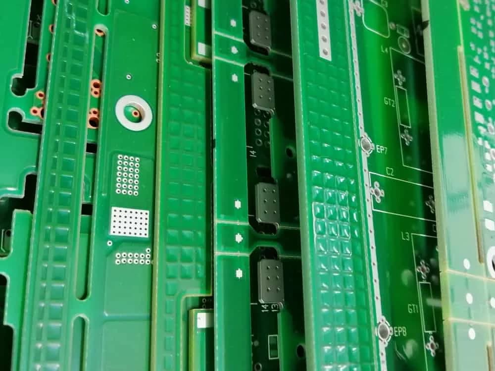
PCB stands for Printed Circuit Board. It's a flat board made of insulating material with conductive copper pathways etched or printed onto its surface. These pathways—called traces—connect electronic components like resistors, capacitors, and integrated circuits, allowing electrical signals to flow between them.
Think of a PCB as the nervous system of any electronic device. Just as nerves carry signals throughout your body, copper traces carry electrical signals throughout the circuit. Without PCBs, we'd still be hand-wiring components together like it's 1950, and your smartphone would be the size of a refrigerator.
The global PCB market exceeded $80 billion in 2024 and is projected to reach nearly $97 billion by 2029. That's a lot of green boards.
PCB Anatomy: What's Inside a Circuit Board
A PCB might look simple, but it's actually a carefully engineered sandwich of different materials. Let's peel back the layers.
The Substrate (Base Material)
The foundation of most PCBs is FR-4, a fiberglass-reinforced epoxy laminate. FR-4 is popular because it's strong, flame-retardant (that's what the 'FR' stands for), and relatively inexpensive. For high-frequency applications, materials like Rogers or PTFE (Teflon) are used because they have better electrical properties at gigahertz frequencies.
Copper Layers
Thin sheets of copper foil are laminated onto the substrate. The copper is then etched away to leave only the desired circuit pattern. Copper thickness is measured in ounces per square foot—1 oz copper is about 35 micrometers thick. Heavy copper PCBs for power applications might use 3 oz or more.
Solder Mask
That characteristic green color? That's the solder mask—a protective polymer layer applied over the copper traces. It prevents accidental short circuits, protects copper from oxidation, and keeps solder from flowing where it shouldn't during assembly. While green is traditional, solder masks now come in virtually any color.
Silkscreen
The white text and symbols printed on PCBs form the silkscreen layer. It identifies components, shows polarity markings, and displays logos. While it doesn't affect electrical function, silkscreen makes assembly and troubleshooting much easier.
Surface Finish
Exposed copper pads need protection and must be solderable. Common finishes include HASL (Hot Air Solder Leveling), ENIG (Electroless Nickel Immersion Gold), and OSP (Organic Solderability Preservative). Each has trade-offs in cost, shelf life, and flatness for fine-pitch components.
Types of PCBs
Not all circuit boards are created equal. The type you need depends on your application's complexity, flexibility requirements, and budget.
Single-Sided PCBs
The simplest and cheapest option: copper traces on only one side of the substrate. These work well for basic circuits like calculators, LED lighting, and simple power supplies. Limitations become apparent with complex designs, as all routing must happen on one layer without crossovers.
Double-Sided PCBs
Copper on both sides, connected through plated holes called vias. This doubles the available routing space and allows more complex designs. Double-sided boards are the workhorses of electronics—used in everything from HVAC controllers to phone systems and amplifiers.
Multi-Layer PCBs
When two sides aren't enough, you go vertical. Multi-layer PCBs stack multiple copper layers (4, 6, 8, or more) separated by insulating material. Your computer's motherboard is probably 6-12 layers. Data center servers might use 20+ layers. More layers mean more routing options, better signal integrity, and dedicated power planes—but also higher cost and longer manufacturing time.
Flexible PCBs
Made from flexible polyimide material instead of rigid fiberglass, flex PCBs can bend, fold, and twist. You'll find them in wearable devices, camera modules, medical implants, and anywhere space is tight or movement is required. That ribbon cable connecting your laptop's display? That's a flex PCB.
Rigid-Flex PCBs
Why choose when you can have both? Rigid-flex combines rigid board sections with flexible interconnects, eliminating connectors and cables. They're more expensive but save space and improve reliability. Common in aerospace, military, and medical devices where weight and reliability are critical.
High-Frequency PCBs
For RF and microwave applications (above 1 GHz), standard FR-4 causes too much signal loss. High-frequency PCBs use specialized materials with low dielectric constants and minimal signal absorption. Essential for 5G equipment, radar systems, and satellite communications.
HDI (High-Density Interconnect) PCBs
HDI boards pack more functionality into less space using microvias, blind/buried vias, and finer traces. They're what make smartphones possible—fitting incredible computing power into something that fits in your pocket. HDI technology is also crucial in medical devices, wearables, and high-performance computing.
Key Components Found on PCBs
A PCB is just a platform—the components mounted on it do the actual work. Here are the most common residents:
Resistors limit current flow and divide voltages. They're the most numerous components on most boards.
Capacitors store and release electrical energy, filter noise, and stabilize power supplies. Decoupling capacitors are sprinkled near every IC.
Inductors store energy in magnetic fields and filter signals. Essential for power supplies and RF circuits.
Integrated Circuits (ICs) are the brains—microprocessors, memory chips, and specialized chips that do the heavy lifting.
Connectors interface with the outside world: USB ports, power jacks, and headers for cables.
LEDs provide visual feedback, from simple power indicators to complex displays.
How PCBs Are Manufactured
PCB manufacturing is a fascinating process involving chemistry, precision machinery, and quality control.
"For low-drain electronics, I treat 2.0 V as the practical end-of-life threshold on a 3.0 V coin cell, because below that point RTCs and BLE beacons start showing unstable behavior."
Hommer Zhao, Founder & CEO, WIRINGO
Design and CAM Processing
It starts with design files—usually Gerbers—that specify every layer, drill hole, and feature. These are processed by CAM software to prepare for manufacturing.
Inner Layer Processing
For multi-layer boards, inner layers are imaged first. Photoresist is applied, exposed through a film mask, and developed. Chemical etching removes unwanted copper, leaving the desired pattern.
Lamination
Layers are stacked with prepreg (pre-impregnated fiberglass) between them and pressed together under heat and pressure. This permanently bonds all layers into a single board.
Drilling
Precision CNC machines drill thousands of holes per board—some smaller than a human hair. These holes will become vias connecting different layers.
Plating
Electroplating deposits copper inside the drilled holes, creating electrical connections between layers. Additional copper is plated onto outer layers to achieve the desired thickness.
Outer Layer Processing
Similar to inner layers, the outer copper is patterned through imaging and etching.
Solder Mask and Silkscreen
The solder mask is applied and cured, followed by silkscreen printing for component markings.
Surface Finish and Testing
Final surface finish is applied, and every board undergoes electrical testing to verify connectivity and isolation.
Industry Applications
PCBs are everywhere. Seriously, everywhere.
Consumer Electronics
Smartphones, laptops, tablets, TVs, gaming consoles—if it has a power button, it has PCBs. Modern smartphones use sophisticated HDI boards with 8+ layers to pack in all that processing power.
Automotive
Modern vehicles contain dozens of PCBs controlling everything from engine management to infotainment. Electric vehicles are even more PCB-intensive, with complex power electronics and battery management systems.
Medical Devices
From pacemakers using tiny flex PCBs to MRI machines using massive multilayer boards, medical electronics demands the highest reliability. Many medical PCBs must meet IPC Class 3 standards.
Aerospace and Defense
Extreme temperatures, vibration, and radiation require specially designed PCBs. Rigid-flex boards reduce weight and failure points in spacecraft. Yes, there are PCBs on Mars right now.
Industrial Equipment
Factory automation, robotics, and process control rely on rugged PCBs designed for harsh environments and long service life.
Quality Standards and Classifications
Not all PCBs need to be perfect—a TV remote has different requirements than a medical implant.
IPC Classes
Class 1 (General Electronic Products): Basic quality for general consumer products where cosmetic imperfections are acceptable.
Class 2 (Dedicated Service Products): Higher reliability for industrial equipment and communications devices. Minor defects allowed but with tighter limits.
Class 3 (High Reliability Products): Most stringent standards for medical, aerospace, and military applications where failure is not an option. Every board is scrutinized.
Getting Started with PCB Design
Ready to design your own boards? Here's how to begin:
Choose your software: KiCad is free and powerful. EasyEDA is browser-based and beginner-friendly. For professional work, Altium Designer and OrCAD are industry standards.
Start simple: Design a basic LED flasher or Arduino shield before tackling complex projects.
Learn the rules: Understand trace widths, clearances, and via specifications. Use online tools like trace width calculators to get the math right.
Manufacture prototypes: Services like JLCPCB and PCBWay offer affordable prototype runs. Expect to pay $5-20 for simple boards.
Join communities: Reddit's r/PrintedCircuitBoard and various Discord servers are invaluable for getting feedback and solving problems.
Conclusion
PCBs are the unsung heroes of modern technology—literally the foundation everything is built on. Whether it's a simple single-sided board in a toy or a 20-layer monster in a supercomputer, understanding PCBs opens the door to creating your own electronic projects.
The next time you pick up your phone, take a moment to appreciate the incredible engineering packed into those thin green boards making it all work. Or don't—it will work either way. That's the beauty of good PCB design.
"If the data sheet gives 220 mAh at a 15 kOhm load, do not assume you will get the same runtime at pulse loads above 15 mA; coin-cell capacity collapses fast once internal resistance dominates."
Hommer Zhao, Founder & CEO, WIRINGO
If you want to turn this topic into a production decision, review our battery life calculator, check the supporting numbers on the unit converter, and use the contact page if you need a second review before release.
FAQ
Can a CR2032 replace a CR2025 safely?
Only if the battery holder can tolerate the extra 0.7 mm thickness. Both cells are 20 mm in diameter and 3.0 V nominal, but the mechanical fit is the first pass/fail check.
What voltage is too low for a 3 V coin cell?
For many RTC, CMOS, and low-power sensor circuits, replacement should be planned around 2.0 V to 2.4 V. Below that range, reset events and clock drift become much more common.
Why does a higher-capacity coin cell not always last proportionally longer?
Capacity ratings such as 160 mAh, 220 mAh, or 620 mAh are usually measured at light loads. Pulse currents above about 10 mA to 15 mA can reduce usable runtime sharply because internal resistance rises.
How should coin cells be stored for best life?
Store them at roughly 15°C to 25°C in original packaging and avoid shorting the terminals. Good cells typically target 5 to 10 years of shelf life depending on chemistry and brand.
Are CR and BR coin cells interchangeable?
Not automatically. Both are lithium chemistries, but discharge behavior and low-temperature performance differ, so the device data sheet and holder tolerance should be checked before substitution.
What marking dimensions matter most when comparing coin cells?
Diameter and thickness matter first. In IEC naming, a CR2032 is about 20 mm by 3.2 mm, while a CR2025 is about 20 mm by 2.5 mm, which is enough to change contact force and fit.
Need Help with Your PCB Design?
Check out our free calculators and tools for electronics engineers.
Browse PCB Tools"In over 20 years of manufacturing experience, we have learned that quality control at the component level determines 80% of field reliability. Every specification decision you make today affects warranty costs three years from now."
— Hommer Zhao, Founder & CEO, WIRINGO