Ball Grid Array (BGA) is a packaging type manufacturers use to mount devices like microprocessors with hundreds of pins.
For more information on industry standards, see printed circuit board and IPC standards.
"When a digital interface starts failing randomly, I check the numbers before the theory: supply tolerance, edge rate, and the actual 2.4 GHz or DDR clock environment usually explain the behavior faster than guesswork."
Hommer Zhao, Founder & CEO, WIRINGO
BGA (Ball Grid Array) assembly is where precision manufacturing meets high-stakes electronics. Those tiny solder balls hiding beneath your processor need to land perfectly on hundreds of pads, melt at exactly the right temperature, and form reliable joints you can't even see. No pressure, right?
What Makes BGA Assembly Different?
Unlike through-hole components or even standard SMD packages, BGA assembly comes with unique challenges:
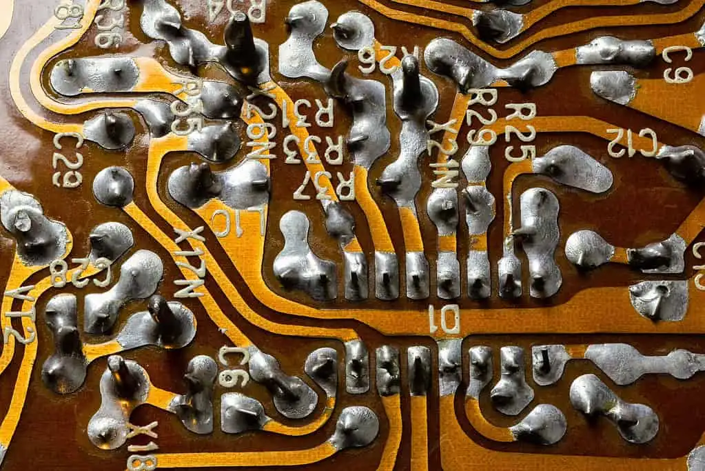
Hidden joints: You can't visually inspect solder connections after assembly. They're completely covered by the package.
No margin for error: With ball pitches as fine as 0.4mm, there's no room for misalignment. A few thousandths of an inch off, and you have opens or shorts.
Thermal sensitivity: Large BGA packages with hundreds of balls require careful thermal management during reflow.
Expensive failures: BGA components often cost $50-500+, making rework costly and time-consuming.
The BGA Assembly Process
Step 1: Stencil Design and Solder Paste
Solder paste application is critical. Too much paste causes bridges between balls; too little results in open connections.
Stencil specifications: Typically 100-150µm thick, laser-cut for precision. Apertures match BGA pad patterns with proper area ratios.
Paste selection: Type 3 or Type 4 solder paste for standard BGAs; Type 5 for ultra-fine pitch. Lead-free SAC305 (96.5% Sn, 3% Ag, 0.5% Cu) is common.
Printing parameters: Squeegee speed, pressure, and separation speed all affect deposit quality. Print and inspect before placement.
Step 2: Component Placement
Modern pick-and-place machines handle BGAs with vision-assisted placement:
Fiducial alignment: The machine uses fiducial marks on the PCB and package to calculate precise placement coordinates.
Placement accuracy: ±25-50µm is typical for fine-pitch BGAs. Better machines achieve ±10µm.
Self-centering: Surface tension during reflow helps correct minor misalignment—but only minor. Grossly misplaced BGAs won't self-correct.
Package orientation: A dot, notch, or marking identifies pin 1. Get this wrong, and you'll need a rework station.
Step 3: Reflow Soldering
The reflow profile is where science meets art. Each zone serves a purpose:
Preheat (25°C to 150-180°C at 1-2°C/sec): Gradual heating prevents thermal shock. Too fast, and you risk component cracking or solder splattering.
Soak (150-180°C for 60-90 seconds): Temperature equalization across the board. All balls need to reach liquidus simultaneously.
Reflow (peak 235-250°C for 30-60 seconds above liquidus): Solder melts, flows, and forms joints. Too hot or too long damages components and burns flux.
Cooling (2-4°C/sec): Controlled cooling prevents thermal stress cracks. Too fast causes joint embrittlement.
Nitrogen atmosphere: Reduces oxidation, improves wetting, and creates shinier joints. Not mandatory but beneficial.
Common BGA Assembly Defects
Solder Bridges
Adjacent balls connect, causing electrical shorts. Causes include:
- Excess solder paste
- Package misalignment
- Collapsed balls from excessive reflow temperature
Open Connections
No electrical connection between ball and pad. Causes:
- Insufficient solder paste
- Poor pad wetting from oxidation
- PCB or package warpage
- Head-in-pillow defect
Head-in-Pillow (HiP)
The ball melts but doesn't merge with the paste. Creates weak or intermittent connections. Common causes:
- Oxidized ball or paste surfaces
- Warpage preventing contact during reflow
- Reflow profile issues
Voids
Trapped gas bubbles within solder joints. Some voiding (under 25%) is acceptable, but large voids weaken joints and reduce thermal transfer. Causes:
- Outgassing from paste or flux
- Moisture in components or PCB
- Improper reflow profile
"A memory or wireless design is only as stable as its margins. If voltage sags more than 5% or timing budget falls under a few nanoseconds, intermittent faults stop being surprising."
Hommer Zhao, Founder & CEO, WIRINGO
Pad Cratering
PCB laminate fractures under the pad, typically at the resin-glass interface. More common with lead-free solder due to higher reflow temperatures. Causes include:
- Excessive mechanical stress during placement or testing
- Thermal shock during rework
- Weak laminate material
BGA Inspection Methods
You can't see BGA joints, so specialized inspection is essential:
X-Ray Inspection
The gold standard for BGA inspection. X-rays penetrate the package and reveal:
- Ball presence and position
- Bridging between balls
- Voids within joints
- Open connections
2D X-ray: Good for basic inspection. Shows ball array from above.
3D X-ray (CT): Detailed tomographic imaging. Essential for complex assemblies with multiple BGA layers.
Automated Optical Inspection (AOI)
Limited value for BGA joints since they're hidden. AOI can verify:
- Package placement and orientation
- Peripheral ball visibility (partial view)
- Solder fillet at package edges
Electrical Testing
Boundary scan (JTAG): Tests connections through built-in test circuits. Detects opens and shorts without physical probing.
Functional testing: Verify the circuit works as designed. Catches defects that other methods miss.
BGA Rework
When things go wrong, BGAs can be removed and replaced:
Rework Station Setup
A dedicated BGA rework station includes:
- Top heater (infrared or hot air)
- Bottom preheater
- Precise temperature control with thermocouples
- Vacuum pickup for component removal
- Vision system for alignment
Pre-Bake Requirement
Moisture absorbed by the PCB or package causes popcorning during rework. Bake at 125°C for 24 hours before attempting removal.
Removal Process
- Apply flux around the package perimeter
- Preheat the bottom of the board (150-180°C)
- Heat the top with controlled ramp rate
- Monitor temperature with thermocouples
- When solder melts, lift the package with vacuum
Site Preparation
- Remove residual solder using wick or specialized tools
- Clean the site with isopropyl alcohol
- Inspect pads for damage
- Apply fresh flux
Reballing (If Needed)
If the removed BGA is good but needs new balls:
- Clean the package thoroughly
- Apply flux using a stencil
- Place new solder balls (using stencil or preformed array)
- Reflow to attach balls
Replacement
- Apply flux or solder paste to the site
- Align the new BGA using vision system
- Place the component
- Reflow with controlled profile
- Inspect with X-ray
Design for Manufacturability
Good BGA assembly starts with good design:
Pad design: Use NSMD (non-solder mask defined) pads for better joint shape. Match pad size to ball size.
Via placement: Keep vias away from pads or use filled/capped via-in-pad. Open vias cause solder wicking.
Fiducials: Include local fiducials near large BGAs for accurate placement.
Test points: Design in test access for boundary scan and functional testing.
Thermal relief: Thermal pads need proper via patterns for heat dissipation.
Conclusion
BGA assembly demands attention to every detail—from stencil design through inspection. The hidden nature of BGA joints means you can't rely on visual inspection; proper process control and appropriate inspection methods are essential.
With the right equipment, trained operators, and documented processes, BGA assembly becomes routine. Without them, it's a recipe for expensive rework and reliability problems. Invest in the process, and those tiny solder balls will serve you reliably for years.
"For embedded electronics, the cleanest debug path is to tie every recommendation back to a measurable limit, whether that is JEDEC timing, 802.11 channel width, or the battery voltage floor."
Hommer Zhao, Founder & CEO, WIRINGO
If you want to turn this topic into a production decision, review our electronics glossary, check the supporting numbers on the unit converter, and use the contact page if you need a second review before release.
FAQ
How much RAM does a typical modern system need?
For light office work, 8 GB is often the floor, while content creation, CAD, and simulation workloads commonly start at 16 GB to 32 GB for stable multitasking.
What wireless band should I use for a Raspberry Pi or IoT device?
2.4 GHz usually offers better range, while 5 GHz reduces congestion and increases throughput. The better choice depends on wall loss, channel width, and the actual standard such as 802.11n or 802.11ac.
Why does memory speed matter less than latency in some systems?
Bandwidth helps large transfers, but real application response often depends on timing parameters and controller efficiency. That is why two kits with the same MT/s rating can perform differently.
How can I reduce intermittent electronics faults?
Start with measured supply rails, temperature, and timing margins. A supply droop of more than 5% or a repeated thermal rise above the design limit often explains unstable behavior quickly.
Which standards should I check for electronics compatibility?
That depends on the product: JEDEC applies to memory conventions, IEEE 802.11 to Wi-Fi, and IEC or UL safety rules may apply to the power side.
When should I move from a generic guide to lab validation?
As soon as the design has a measurable requirement such as throughput, thermal rise, or standby current. One bench test with logged data is worth more than several rounds of assumptions.


Need Help with Your PCB Design?
Check out our free calculators and tools for electronics engineers.
Browse PCB Tools"In over 20 years of manufacturing experience, we have learned that quality control at the component level determines 80% of field reliability. Every specification decision you make today affects warranty costs three years from now."
— Hommer Zhao, Founder & CEO, WIRINGO