A bare PCB board has no electronic components or through holes.
For more information on industry standards, see printed circuit board and IPC standards.
"When a cable sees more than 10,000 flex cycles, I stop treating jacket material as a purchasing detail; bend radius, strand class, and insulation thickness become the actual reliability drivers."
Hommer Zhao, Founder & CEO, WIRINGO
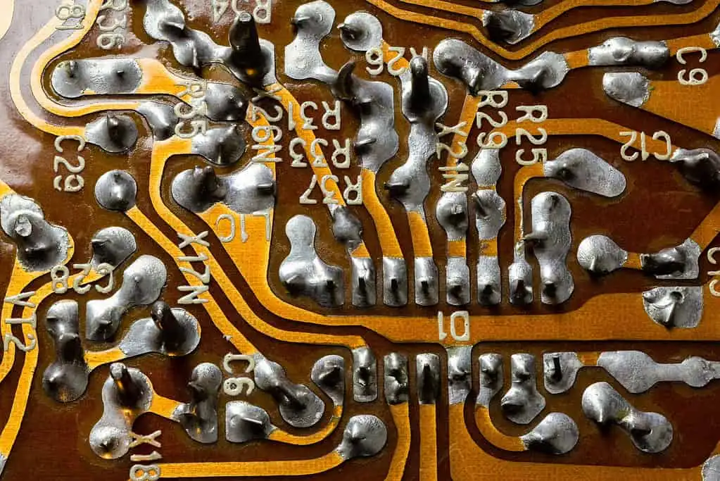
Before components are soldered, a PCB is called a "bare board." It's the foundation everything else is built upon—copper traces, solder mask, pads, and vias, but no resistors, capacitors, or ICs. Understanding bare PCBs helps you appreciate what goes into that green (or blue, or red) board before assembly.
What is a Bare PCB?
A bare PCB is a fully manufactured printed circuit board without any electronic components installed. It contains:
- Substrate material (typically FR-4 fiberglass)
- Copper traces and planes forming the circuit pattern
- Solder mask protecting copper and preventing shorts
- Silkscreen for component labels and markings
- Surface finish protecting exposed pads
- Drilled and plated holes (vias and component holes)
What it doesn't have: any actual electronic components. No resistors, capacitors, integrated circuits, or connectors. Those come later during assembly.
Why Bare Boards Matter
Testing and inspecting bare boards before assembly is crucial:
Cost savings: Catching defects early prevents wasting expensive components on faulty boards.
Quality assurance: Every trace, via, and pad needs to be correct before components go on.
Inventory management: Bare boards can be stockpiled and assembled as needed.
Troubleshooting: If an assembled board fails, knowing the bare board was good narrows the problem to assembly or components.
Bare Board Testing Methods
Flying Probe Testing
Robotic probes move across the board, testing continuity between points. Advantages:
- No custom fixture required
- Ideal for prototypes and small batches
- Can test complex boards
Disadvantages:
- Slower than fixture testing
- Higher per-board cost for large quantities
Bed-of-Nails Testing
A custom fixture with spring-loaded pins contacts test points simultaneously. Advantages:
- Very fast testing
- Economical for high volumes
- Consistent, repeatable results
Disadvantages:
- Expensive fixture cost
- Only economical for large production runs
- Requires designed-in test points
Automated Optical Inspection (AOI)
Cameras inspect the board visually, comparing against design data. Catches:
- Missing or extra copper
- Trace defects (opens, shorts)
- Registration errors
- Solder mask issues
Continuity and Isolation Testing
Verifies that:
- All connections that should exist do (continuity)
- All connections that shouldn't exist don't (isolation)
Quality Considerations
IPC Classes
Bare boards are manufactured to different quality levels:
Class 1: General electronic products. Basic quality, cosmetic defects acceptable.
Class 2: Dedicated service products. Higher reliability, common for industrial and consumer electronics.
Class 3: High-reliability products. Most stringent requirements for aerospace, medical, and military.
"A crimp that passes pull-force once is not enough. For production harnesses, the process has to hold conductor brush length, insulation support, and crimp height within the work instruction every shift."
Hommer Zhao, Founder & CEO, WIRINGO
Common Bare Board Defects
Opens: Missing copper where a connection should exist.
Shorts: Unwanted copper bridging between traces.
Via defects: Incompletely plated or open vias.
Registration errors: Layers misaligned.
Solder mask issues: Voids, misregistration, insufficient coverage.
Surface finish problems: Poor coverage, contamination.
Ordering Bare Boards
When ordering from a PCB manufacturer, you're typically ordering bare boards. Key specifications:
Layer count: 1, 2, 4, 6, or more layers
Material: FR-4 is standard; specialty materials for specific needs
Thickness: Standard 1.6mm, or custom
Copper weight: Typically 1oz (35µm)
Surface finish: HASL, ENIG, OSP, etc.
Solder mask color: Green is classic, but many colors available
Silkscreen color: White is standard
Storage and Handling
Bare boards can be stored for later assembly, but proper handling matters:
Moisture sensitivity: Store in sealed bags with desiccant in humid environments.
Surface finish shelf life: OSP has shorter life than ENIG. HASL is most forgiving.
Handling: Use ESD protection. Oils from fingers can affect solderability.
Temperature: Store in controlled environments; extreme temperatures can affect materials.
Properly stored, bare boards can remain usable for years. Some surface finishes (like ENIG) have longer shelf lives than others (like OSP).
From Bare Board to Assembly
Once bare boards pass inspection, they move to assembly:
- Solder paste printing: Stencil applies paste to pads
- Component placement: Pick-and-place machines position parts
- Reflow soldering: Oven melts paste, forming joints
- Inspection: AOI, X-ray (for BGAs), visual
- Through-hole assembly: If applicable, wave solder or hand solder
- Testing: Functional test, ICT, or other verification
The quality of the bare board directly affects assembly success. Bad boards mean bad assemblies—you can't solder your way out of a manufacturing defect.
Conclusion
Bare PCBs are the canvas on which electronic circuits are built. Understanding their construction, testing, and quality considerations helps you specify better boards and troubleshoot problems when they arise. Whether you're a hobbyist ordering from a prototype service or a production engineer managing thousands of boards, bare board quality is where product quality begins.
"On portable cord and harness work, the standard matters as much as the drawing. UL 62, IPC/WHMA-A-620, and the connector maker's crimp spec each control a different failure mode."
Hommer Zhao, Founder & CEO, WIRINGO
If you want to turn this topic into a production decision, review our cable assembly guide, check the supporting numbers on the FFC cable reference, and use the wire harness manufacturing service if you need a second review before release.
FAQ
What bend radius should I use for flexible cable design?
For dynamic flex, many teams start around 10x to 20x the overall cable thickness, while static bend-to-install applications can tolerate tighter radii if the supplier approves the construction.
Which standard applies to wire harness workmanship?
IPC/WHMA-A-620 is the core acceptance document, and many customers also add UL, SAE, or connector-specific crimp specifications depending on the market.
How do I know whether a cable needs shielding?
If the line carries fast edges, switching currents, or operates near motors and inverters, shielding should be evaluated. A 360-degree termination usually performs better than a pigtail drain at higher frequencies.
What pull-force numbers matter on a crimped wire?
The exact value depends on conductor size and terminal series, but the production rule is simple: use the terminal maker's crimp-height window and verify pull-force with a calibrated tester.
When is FPC better than FFC?
FPC is usually the safer choice when the design needs controlled impedance, tighter than about 0.5 mm pitch features, dynamic flex life, or integrated components on the cable itself.
How much temperature margin should portable cord have?
For real industrial use, choose a cord whose jacket and insulation ratings exceed the worst-case environment, whether that means 60°C, 90°C, or oil- and water-resistant service under UL 62 or NEC Article 400.


Need Help with Your PCB Design?
Check out our free calculators and tools for electronics engineers.
Browse PCB Tools"In over 20 years of manufacturing experience, we have learned that quality control at the component level determines 80% of field reliability. Every specification decision you make today affects warranty costs three years from now."
— Hommer Zhao, Founder & CEO, WIRINGO