Complete guide to PCB assembly and manufacturing. Learn about SMT vs through-hole technology, the step-by-step assembly process, testing methods, and design for manufacturing best practices.
For more information on industry standards, see printed circuit board and IPC standards.
"If your design needs controlled impedance, length matching, and production release data, the real threshold is not price but output quality; a tool that cannot generate verified Gerber, drill, and pick-and-place files will cost more than a $300 monthly license."
Hommer Zhao, Founder & CEO, WIRINGO
That circuit board design sitting in your CAD software looks perfect. The schematic checks out, the layout passes DRC, and the Gerbers are ready. But how does it become an actual working product? Understanding the PCB assembly process helps you design boards that manufacture smoothly and perform reliably.
This guide walks through every step of PCB assembly, from bare board to tested product.
PCB Fabrication vs Assembly: Understanding the Difference
Before diving into assembly, let's clarify terminology that often confuses newcomers.
PCB Fabrication: Creating the bare circuit board itself—the substrate with copper traces, drilled holes, solder mask, and silkscreen. You send Gerber files; you receive boards ready for components.
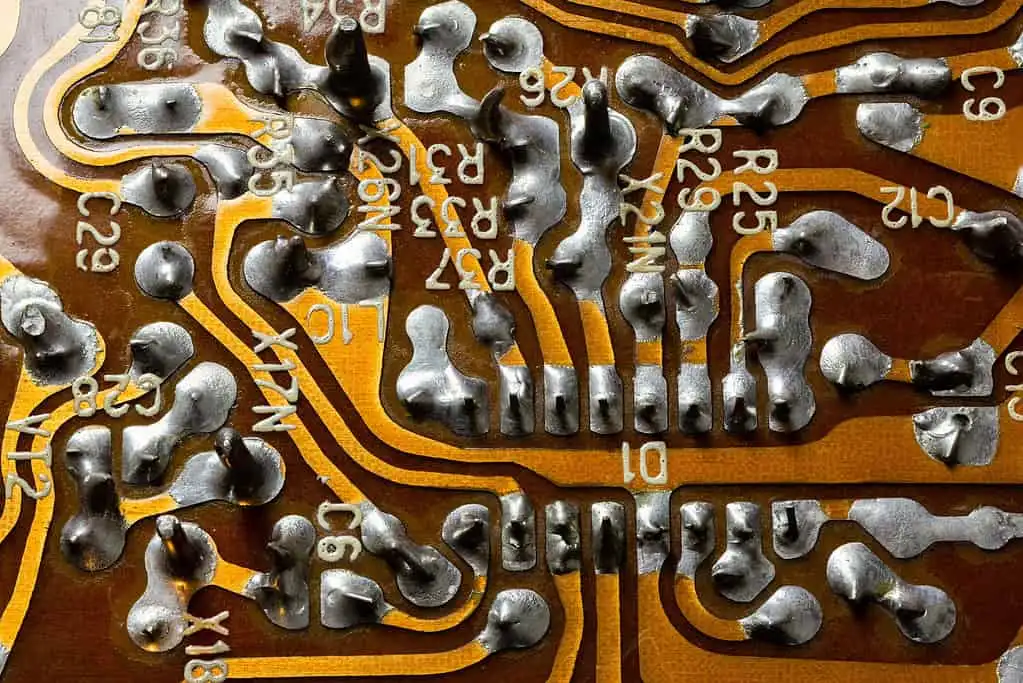
PCB Assembly (PCBA): Populating that bare board with components—resistors, capacitors, ICs, connectors. You receive functional circuit board assemblies.
Many manufacturers offer both services together as "turnkey" manufacturing. Others specialize in one or the other. Either way, both processes must succeed for a working product.
The Two Assembly Technologies: SMT vs Through-Hole
Modern PCBs use two fundamental component mounting approaches, often combined on the same board.
Surface Mount Technology (SMT)
Surface mount components sit directly on the board surface, soldered to pads without leads passing through holes. SMT dominates modern electronics because:
- Smaller components: 0201 packages measure just 0.6mm × 0.3mm
- Higher density: Both sides of the board can hold components
- Faster assembly: Automated pick-and-place machines handle thousands of parts per hour
- Better high-frequency performance: Shorter leads mean less inductance
Through-Hole Technology (THT)
Through-hole components have leads that pass through holes in the PCB and solder on the opposite side. Despite being older technology, THT remains essential for:
- Mechanical strength: Connectors under physical stress
- High power: Components needing better thermal dissipation
- Easy prototyping: Hand soldering is straightforward
- Reliability: Military and aerospace applications demanding maximum durability
Most boards use mixed technology—SMT for the majority of components with through-hole for connectors, power devices, and anything requiring mechanical robustness.
SMT Assembly Process: Step by Step
SMT assembly follows a precise sequence that transforms bare boards into populated assemblies in minutes.
Step 1: Solder Paste Printing
The process begins with applying solder paste to the PCB pads. A stainless steel stencil with laser-cut openings aligns over the board. A squeegee blade pushes solder paste across the stencil, forcing paste through the openings onto the pads below.
Solder paste is a carefully formulated mixture of tiny solder spheres (typically 25-45 microns diameter) suspended in flux. The flux cleans oxide from pads and pins, enabling reliable solder joints.
Critical factors:
- Stencil thickness affects paste volume (thicker = more paste)
- Aperture design must match pad geometry
- Squeegee pressure, speed, and angle require optimization
- Paste temperature affects printing consistency
A good paste print is essential—most SMT defects trace back to printing problems.
Step 2: Solder Paste Inspection (SPI)
Before placing components, automated inspection verifies the paste print. 3D SPI machines measure:
- Volume: Is enough paste on each pad?
- Height: Is paste thickness consistent?
- Area: Does paste coverage match the aperture?
- Position: Is paste centered on the pad?
Catching printing defects before component placement saves the cost of processing bad boards through the entire line.
Step 3: Pick and Place
Pick-and-place machines are the workhorses of SMT assembly. These remarkable machines:
- Pick components from reels, trays, or tubes using vacuum nozzles
- Center the component using vision systems
- Rotate to correct orientation
- Place precisely on the solder paste with controlled force
Modern pick-and-place machines achieve stunning speed—placing 100,000+ components per hour. Vision systems verify correct parts and orientation, rejecting components that don't match.
Multiple placement heads and feeders allow different component types to load simultaneously. Setup time (loading feeders with correct reels) often exceeds actual placement time for small runs.
Step 4: Pre-Reflow Inspection (Optional)
Some lines include automated optical inspection (AOI) before reflow to catch placement errors while correction is still easy. A misplaced component before soldering can simply be repositioned; after soldering, rework becomes necessary.
Step 5: Reflow Soldering
The assembled board passes through a reflow oven—essentially a precisely controlled tunnel of heat. The temperature profile includes:
- Preheat zone: Gradually raises temperature, activating flux
- Thermal soak: Equalizes temperature across the board
- Reflow zone: Exceeds solder melting point (~217°C for lead-free)
- Cooling zone: Solidifies solder joints
The profile balances multiple requirements: reaching reflow temperature without thermal shock, keeping components within their temperature ratings, allowing flux to clean surfaces before solder melts, and cooling fast enough to form proper grain structure.
Lead-free solders require higher temperatures than traditional tin-lead, making thermal management more challenging.
Step 6: Post-Reflow Inspection
Automated Optical Inspection (AOI) examines every solder joint and component. Cameras capture high-resolution images, and software algorithms detect:
- Missing components
- Misaligned components
- Solder bridges (shorts between pads)
- Insufficient solder
- Tombstoning (component standing on end)
- Polarity errors on marked components
For BGA packages where joints hide under the component, X-ray inspection reveals hidden defects.
Through-Hole Assembly Process
Through-hole components follow a different path, often after SMT is complete on boards using both technologies.
Manual Insertion
"For teams designing 6-layer and 8-layer boards, library control and DRC rule coverage matter more than UI polish, because one missed clearance rule can burn a full prototype spin."
Hommer Zhao, Founder & CEO, WIRINGO
For low volumes or complex assemblies, operators hand-insert through-hole components. This approach offers flexibility but depends on operator skill and attention.
Best practices:
- Follow a logical insertion sequence (low components first)
- Verify component values and orientations
- Form leads appropriately before insertion
- Check proper seating after insertion
Automated Insertion
For higher volumes, axial and radial insertion machines automatically place common through-hole components like resistors and capacitors. Specialized machines handle odd-form components like connectors and relays.
Wave Soldering
The classic through-hole soldering method sends boards over a wave of molten solder. The board passes over a continuously pumped wave that contacts the bottom surface, wetting leads and pads while solder mask prevents bridging.
Wave soldering efficiently solders all through-hole components simultaneously but requires careful setup:
- Conveyor speed affects heat transfer
- Wave height must contact leads without flooding pads
- Preheat prevents thermal shock
- Flux application ensures clean surfaces
Selective Soldering
Modern mixed-technology boards often use selective soldering instead of wave soldering. A programmable nozzle applies solder only to through-hole locations, avoiding damage to adjacent SMT components already soldered.
Selective soldering is slower than wave soldering but offers precision impossible with full-board wave exposure.
Mixed Technology Assembly
Real-world boards rarely use pure SMT or pure through-hole. The typical mixed-technology sequence:
- SMT side one: Print, place, reflow the primary SMT side
- SMT side two (if double-sided): Flip, print, place, reflow the secondary side
- Through-hole: Insert through-hole components
- Final soldering: Wave or selective solder the through-hole joints
- Inspection and test: Verify the complete assembly
Thermal budgeting becomes critical—components experience heat during each reflow and soldering step. The total thermal exposure must stay within limits.
Testing and Quality Assurance
Assembly isn't complete until the board proves functional.
In-Circuit Test (ICT)
Bed-of-nails fixtures make contact with test points across the board. ICT verifies:
- Component presence and values
- Solder joint integrity
- Short circuits
- Open circuits
ICT catches manufacturing defects efficiently but requires expensive custom fixtures for each board design.
Flying Probe Test
Instead of fixed test points, moving probes contact locations across the board. Flying probe is slower than ICT but requires no custom fixtures—ideal for prototypes and low volumes.
Functional Test
The ultimate verification: does the board work as designed? Functional test applies power and signals, verifying correct operation. This catches design errors that pass ICT and defects that electrical tests miss.
Burn-In Test
For high-reliability applications, extended operation at elevated temperature stresses components. Infant mortality failures occur early; surviving units prove themselves before shipping.
Design for Manufacturing (DFM) Considerations
Smart designers consider assembly during layout, not after.
Component Selection
- Prefer standard package sizes with good availability
- Match package thermal requirements to assembly capability
- Consider lead-free compatibility for all components
- Avoid mixing fine-pitch and coarse-pitch on the same board when possible
Pad Design
- Follow component manufacturer recommendations
- Include solder thieves for unbalanced pads (preventing tombstoning)
- Size thermal pads for proper heat dissipation during soldering
- Ensure consistent pad sizes within component families
Spacing and Clearance
- Maintain minimum spacing for stencil wall integrity
- Allow room for rework access
- Consider pick-and-place nozzle clearance
- Keep tall components away from edges
Fiducials and Tooling
- Include global fiducials for board alignment
- Add local fiducials near fine-pitch components
- Design tooling holes for fixturing
- Mark board edges clearly for depanelization
Choosing an Assembly Partner
Whether prototype or production, your assembly partner significantly affects success.
For prototypes:
- Quick-turn capability matters most
- NRE (non-recurring engineering) charges should be reasonable
- Engineering support helps catch issues early
For production:
- Capacity must match your volume requirements
- Quality certifications (ISO, AS9100, etc.) indicate process maturity
- Supply chain management reduces your logistics burden
- Geographic location affects shipping cost and communication
Common Assembly Defects and Prevention
Understanding failure modes helps you design boards that avoid them.
| Defect | Cause | Prevention |
|---|---|---|
| Solder bridges | Excess paste, poor stencil design | Proper aperture sizing |
| Tombstoning | Unequal heat or paste distribution | Symmetric pad design |
| Cold joints | Insufficient heat | Proper thermal profiling |
| Voids | Outgassing during reflow | Thermal soak optimization |
| Component shift | Excessive reflow temperature | Profile optimization |
The Bottom Line
PCB assembly transforms your design from concept to reality. Understanding the process helps you design boards that assemble smoothly, catch problems before they become expensive, and communicate effectively with your manufacturing partners.
Whether you're building one prototype or a million production units, the fundamentals remain the same: good design enables good manufacturing. Master both, and your products will succeed.
"I look for three outputs before I trust any PCB CAD flow: netlist consistency, manufacturing outputs checked against IPC naming conventions, and a 3D review that catches connector interference before release."
Hommer Zhao, Founder & CEO, WIRINGO
If you want to turn this topic into a production decision, review our EDA comparison reference, check the supporting numbers on the EDA shortcuts reference, and use the contact page if you need a second review before release.
FAQ
What features matter most in PCB layout software?
For professional work, the short list is controlled-rule DRC, multi-layer stackup support, 3D clearance review, and manufacturing outputs such as Gerber X2, drill files, and pick-and-place exports.
Is free PCB design software good enough for a real product?
It can be for 2-layer or moderate 4-layer designs, but once the board reaches fine-pitch BGAs, impedance control, or dense library management, commercial tools usually save at least one prototype spin.
How many layers can entry-level tools handle reliably?
Many can draw 4-layer and even 6-layer boards, but the real limit is rule management and verification quality, not the raw layer count shown in marketing.
What file outputs should I verify before sending a board to fabrication?
At minimum, review Gerber or ODB++, NC drill, stackup notes, assembly drawings, and BOM outputs. A missing polarity mark or drill map can delay production by days.
Why is library control such a big deal in EDA tools?
A footprint error of even 0.2 mm can be enough to cause tombstoning, insufficient heel fillet, or connector interference. Centralized libraries reduce that risk across every release.
How should a team compare EDA tools objectively?
Use the same test design, then score routing speed, DRC coverage, library workflow, and manufacturing output accuracy. Three trial builds usually reveal more than a feature checklist.


Need Help with Your PCB Design?
Check out our free calculators and tools for electronics engineers.
Browse PCB Tools"In over 20 years of manufacturing experience, we have learned that quality control at the component level determines 80% of field reliability. Every specification decision you make today affects warranty costs three years from now."
— Hommer Zhao, Founder & CEO, WIRINGO