Aluminium PCB Manufacturer
Metal core PCB fabrication with thermal conductivity from 1.0 to 8.0 W/mK, copper weights 1–10 oz, and board thicknesses 0.5–3.2 mm. MOQ 5 panels, lead time from 5 business days, IPC-6012 Class 2/3 compliant with full thermal impedance test reporting.
What Makes Aluminium PCBs Different
An aluminium PCB — also called a metal core PCB, MCPCB, or aluminium clad laminate — replaces the FR-4 substrate with an aluminium alloy base plate. The stackup is straightforward: a copper foil circuit layer on top, a thin thermally conductive but electrically insulating dielectric layer in the middle, and the aluminium base at the bottom. Heat flows through the dielectric into the metal core and out into your heatsink or chassis, instead of being trapped in fiberglass.
And that matters more than most engineers realize. We have seen designs where a high-power LED on FR-4 with eight thermal vias ran at a junction temperature of 128°C — well above the 100°C de-rating threshold for most Cree and Lumileds parts. The same LED on a single-layer aluminium board with 1.5 W/mK dielectric dropped to 74°C. Same footprint, same copper weight, dramatically different thermal outcome. The dielectric layer is the bottleneck, and that is exactly where most suppliers cut corners — using cheaper polymer fills with 0.8 W/mK conductivity instead of the ceramic-loaded materials that hit 3.0+ W/mK.
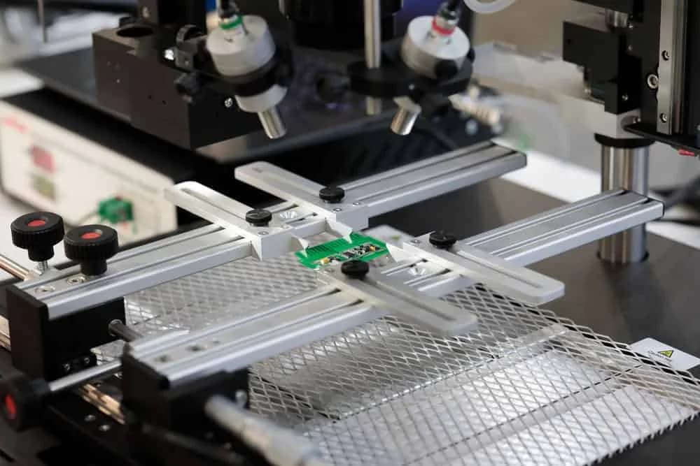
Our factory runs dedicated MCPCB lines, not FR-4 lines repurposed for occasional metal core jobs. That distinction sounds minor. It is not. Aluminium substrates require different drilling parameters (carbide bits at higher RPM, different feed rates), different routing tools (the aluminium base gums up standard FR-4 routing bits), and different lamination pressures. When a shop treats your MCPCB as an afterthought on their FR-4 line, you get inconsistent dielectric thickness, edge burrs on the aluminium, and — the one nobody talks about — delamination during reflow because the CTE mismatch between copper and aluminium was not properly managed in the press cycle.
Manufacturing Capabilities
🔥
Thermal Conductivity
Dielectric layers from 1.0 W/mK (standard polymer) to 8.0 W/mK (ceramic-filled). We publish measured thermal impedance data on every lot — not just the datasheet nominal value. Three conductivity tiers let you trade cost vs. thermal performance precisely.
📐
Layer Configurations
Single-layer (copper/dielectric/aluminium), double-sided with PTH, and multilayer up to 8 layers. Single-layer is the thermal sweet spot — every additional FR-4 prepreg layer between copper and aluminium raises thermal resistance by 20–40%.
⚡
Heavy Copper
Copper weights from 1 oz (35 μm) to 10 oz (350 μm). Heavy copper MCPCBs handle 20+ amp current paths for motor drives and power converters. We etch 10 oz copper with controlled line width tolerance of ±0.15 mm — tighter than the ±0.25 mm most shops quote for heavy copper.
🛡️
Surface Finishes
HASL lead-free, ENIG (3–5 μm Ni / 0.03–0.05 μm Au), OSP, immersion silver, and immersion tin. ENIG is our default recommendation for LED and power applications — flat coplanarity for wire bonding and no thermal degradation after multiple reflow cycles.
📏
Board Dimensions
Maximum panel size 530 × 610 mm (21″ × 24″). Finished board thickness from 0.5 mm to 3.2 mm. Aluminium base thickness options: 0.5 mm, 0.8 mm, 1.0 mm, 1.5 mm, 2.0 mm, 3.0 mm. Thicker bases dissipate more heat but increase routing difficulty and cost.
✅
Compliance & Testing
IPC-6012 Class 2 and Class 3 qualified. Dielectric breakdown tested at 2 kV AC minimum per IPC-6012. Thermal impedance measured per JEDEC JESD51-1. Full test reports shipped with every order.
Aluminium PCB Specifications — How We Compare
Most MCPCB suppliers publish thermal conductivity as a single number. That number is usually the dielectric material's datasheet value — not the measured board-level thermal impedance, which is what actually determines your junction temperature. Below is a parameter-by-parameter breakdown comparing IPC standard requirements, our measured capabilities, and typical industry benchmarks. Pay attention to the dielectric thickness and breakdown voltage rows — those two parameters are where the real reliability risk lives.
| Parameter | IPC Standard | Our Capability | Industry Benchmark |
|---|---|---|---|
| Dielectric Thermal Conductivity | Not specified | 1.0–8.0 W/mK (measured) | 0.8–3.0 W/mK (nominal) |
| Dielectric Thickness | Per IPC-4101 | 75–200 μm (±10 μm) | 75–200 μm (±25 μm) |
| Dielectric Breakdown Voltage | 2 kV AC (Class 2) | 4 kV AC (typical) | 2–3 kV AC |
| Copper Weight Range | 0.5–4 oz (standard) | 1–10 oz | 1–6 oz |
| Heavy Copper Line Width Tolerance | ±0.25 mm | ±0.15 mm | ±0.25 mm |
| Aluminium Base Alloy | Per IPC-4101 | 5052 / 6061-T6 | 5052 only |
| Minimum Board Thickness | 0.8 mm | 0.5 mm | 0.8 mm |
| Thermal Impedance Testing | Not mandated | 100% lots, JEDEC JESD51-1 | Sample or none |
*Industry benchmark data compiled from publicly available specifications of 12 MCPCB suppliers as of Q1 2026. "Nominal" thermal conductivity refers to datasheet values without board-level verification.
How We Build Your Aluminium PCB — Step by Step
The MCPCB fabrication process differs from standard FR-4 at several critical steps. Here is what happens after you submit your Gerber files and BOM, and where the process diverges from what a typical FR-4 shop would do.
1
DFM Review & Thermal Simulation Check
We review your layout for thermal via placement, copper pour coverage on the component side, and dielectric overlap margins. A common mistake we catch: thermal vias placed too close to the board edge where the aluminium base has no mechanical support, causing the drill to break through the dielectric and short to the core. We flag these before production starts. If you provide component power dissipation data, we run a quick thermal resistance estimate — junction-to-substrate — and tell you whether the dielectric conductivity class you selected will keep temperatures in the safe zone. This takes 24 hours and costs nothing.
2
Material Procurement & Incoming Inspection
We stock 5052 and 6061 aluminium cores in standard thicknesses (0.5, 0.8, 1.0, 1.5, 2.0, 3.0 mm) and maintain standing inventory of Bergquist, Laird, and NanYa dielectric laminates. Incoming inspection includes dielectric thickness measurement at 9 points per panel (4 corners, 4 edge midpoints, center) using a micrometer with 1 μm resolution. Panels exceeding ±10 μm dielectric thickness variation are rejected. This is stricter than the ±25 μm tolerance most suppliers accept — but dielectric thickness variation directly translates to thermal resistance hotspots, and we have the data to prove it matters.
3
Imaging, Etching & Copper Patterning
Standard photoimaging and etching for copper weights up to 4 oz. For 6–10 oz heavy copper, we use a modified etch process with longer dwell times and higher spray pressure to achieve ±0.15 mm line width tolerance. The aluminium base acts as a heat sink during etching, which actually helps — it keeps the laminate flat and prevents warpage that plagues heavy-copper FR-4 boards. After etching, we AOI-scan every panel at 100% coverage, not the statistical sampling some shops use.
4
Drilling, Routing & V-Groove Scoring
Drilling through aluminium requires carbide bits at 80–100 kRPM with peck drilling cycles — standard FR-4 drilling parameters will shatter the bit or smear the aluminium into the hole wall. We use dedicated CNC routers with diamond-coated tools for profiling, which produces clean edges without the burrs that standard routing bits leave on aluminium. V-groove scoring (0.3 mm residual thickness) is available for snap-out panelization. We also offer countersunk mounting holes — something many MCPCB shops cannot do because their routing equipment lacks the Z-axis precision for angled cuts on metal.
5
Surface Finish Application
ENIG is our most popular finish for MCPCBs — the electroless nickel layer provides a diffusion barrier that survives multiple reflow cycles without degradation, and the immersion gold cap ensures solderability and wire-bond compatibility. HASL lead-free is available for cost-sensitive applications, though the uneven surface can create tilt issues on large QFN packages. OSP is the budget option but has a 6-month shelf life limit. All finishes are thickness-verified with XRF measurement on every lot.
6
Electrical & Thermal Testing, Final Inspection
Every panel gets 100% electrical testing (open/short on all nets) plus dielectric breakdown verification at 2 kV AC for Class 2 or 3 kV AC for Class 3. Thermal impedance is measured on a sample basis per lot using a transient plane source instrument per JEDEC JESD51-1. We ship the measured thermal resistance value in the test report — not a theoretical calculation, not the material datasheet number, but the actual tested value for your specific lot. If you need 100% thermal testing on every board, we can do that too (add 2 days to lead time).
The Dielectric Layer — Where MCPCBs Live or Die
If there is one section of this page worth reading carefully, it is this one. The dielectric layer in an aluminium PCB serves two conflicting purposes: it must be an excellent electrical insulator (high breakdown voltage, low leakage current) and an excellent thermal conductor (high thermal conductivity, low thermal resistance). No material does both perfectly. Every dielectric is a compromise, and understanding that compromise is the difference between a board that runs cool for years and one that fails in the field after a thermal cycling event.
We offer three dielectric tiers. The standard tier uses a polymer-filled epoxy at 1.0 W/mK thermal conductivity — adequate for low-density LED strips and signage where each LED dissipates under 0.5 W. The mid tier uses ceramic-loaded polymer at 2.0–3.0 W/mK, which is the sweet spot for most high-power LED applications (COB arrays, streetlights, horticulture fixtures). The high tier uses a ceramic-dominant dielectric at 5.0–8.0 W/mK, designed for power electronics — IGBT modules, MOSFET arrays, motor drive inverters — where you need to pull 10+ watts through a small footprint.
But here is the trade-off that datasheets rarely explain: as thermal conductivity goes up, dielectric thickness generally must increase to maintain the same breakdown voltage. Our standard 1.0 W/mK dielectric achieves 4 kV AC breakdown at 75 μm thickness. The 8.0 W/mK dielectric needs 150–200 μm to hit the same breakdown level. Thicker dielectric means higher thermal resistance (Rth = thickness / conductivity), which partially offsets the conductivity gain. The net improvement from 1.0 to 8.0 W/mK is roughly 3–4× in thermal resistance, not 8×. That is still a massive improvement — but only if you account for the thickness change in your thermal model. We provide the actual Rth values for each tier so you can model accurately.
One more thing — and this is the part most guides do not mention — dielectric delamination is the number one failure mode for MCPCBs in the field. It happens when the CTE (coefficient of thermal expansion) mismatch between copper (17 ppm/°C) and aluminium (23 ppm/°C) creates shear stress at the dielectric interface during thermal cycling. Our lamination process uses a ramped pressure profile that holds the press at 180°C for 90 minutes with a controlled cool-down, which produces a bond strength exceeding 1.5 N/mm (measured per IPC-TM-650 2.4.8). Cheap lamination processes skip the controlled cool-down, and the resulting residual stress causes delamination after as few as 50 thermal cycles between -40°C and +125°C. We have tested this ourselves — 500 cycles with zero delamination on our standard process versus delamination starting at cycle 80 on fast-cooled panels.
Design Decisions That Affect Cost and Performance
We have fabricated thousands of aluminium PCB designs over the years, and certain patterns keep showing up — both good and bad. Here are the design decisions that have the biggest impact on whether your board performs well thermally and comes in at a reasonable cost.
Copper Pour Coverage
Fill as much of the top copper layer as possible with solid pour, connected to your thermal pads. Every square millimetre of copper that is not covered by pour is a missed opportunity to spread heat laterally before it reaches the dielectric. We regularly see designs where the copper pour covers only 40% of the board area, with large gaps between component pads. Filling those gaps can reduce peak junction temperature by 5–10°C with zero cost increase. It is free thermal performance.
Thermal Vias — Use Them, But Correctly
On a single-layer MCPCB, thermal vias do not carry heat to the aluminium — the dielectric layer does that directly. Vias are useful on double-sided and multilayer boards where heat needs to travel from an inner layer to the aluminium base. When you do use vias, fill them with copper or epoxy-copper paste. Open vias create solder wicking during assembly that starves the joint. Via diameter should be 0.3–0.5 mm — larger vias waste board area without proportional thermal benefit. We plug vias as a standard step in our process, but if your previous supplier left them open, you probably discovered the solder wicking problem the hard way (ask me how I know — we replaced an entire batch of 200 boards for a customer whose previous vendor skipped via filling).
Aluminium Thickness Selection
Thicker aluminium spreads heat more effectively across the board area, which matters for designs with localized hot spots. But beyond 1.5 mm, the marginal thermal benefit diminishes rapidly while the routing difficulty and cost increase. For most LED applications, 1.0–1.5 mm aluminium is optimal. For power modules with 50+ W dissipation, 2.0–3.0 mm is justified. Going to 3.0 mm aluminium on a 100 mm × 100 mm board adds roughly $2–3 per panel in material cost and requires an extra routing pass — but it can reduce peak substrate temperature by another 8–12°C compared to 1.5 mm.
Single-Layer vs. Multilayer
If your circuit fits on a single layer, keep it there. A single-layer MCPCB has the lowest possible thermal resistance because the dielectric sits directly between the copper and the aluminium. Every additional layer adds FR-4 prepreg and a second dielectric interface. A 4-layer MCPCB typically has 2–3× the thermal resistance of an equivalent single-layer design. The only reasons to go multilayer are routing density (you cannot fit all the traces on one layer) or signal integrity requirements (controlled impedance, EMI shielding). If you must go multilayer, put your highest-power components on the layer closest to the aluminium core.
Where Aluminium PCBs Make the Most Impact
LED Lighting
High-power COB LEDs, streetlights, horticulture fixtures, automotive headlamps, and backlighting units. LED junction temperature directly determines lumen maintenance and lifespan — a 10°C reduction roughly doubles LED life per the L70 degradation model. MCPCBs are the standard thermal solution for any LED dissipating more than 1 W.
Power Conversion
SMPS, DC-DC converters, motor drives, inverter modules. MOSFETs and IGBTs on aluminium substrates run cooler, which reduces RDS(on) drift and extends semiconductor life. Heavy copper (6–10 oz) MCPCBs handle the high-current paths that would require bus bars on FR-4.
Automotive Electronics
LED headlamp drivers, battery management systems, HEV/EV power modules. Automotive under-hood temperatures reach 105°C ambient — the aluminium substrate provides both thermal management and mechanical rigidity that FR-4 cannot match in vibration environments.
RF & Microwave
Power amplifiers, RF transmitters, and base station PA modules. The aluminium base provides a stable ground plane and heat spreading. For RF applications, we offer controlled dielectric constant (εr 4.2–4.8) with ±0.1 tolerance — important for impedance matching on high-frequency traces.
Case Study: High-Power LED Streetlight Module
Challenge
A European lighting OEM needed 12,000 aluminium PCBs for a 200 W COB LED streetlight. Their previous supplier's boards had a 3.2% field failure rate after 12 months — LED modules were overheating, causing premature lumen depreciation and, in some cases, catastrophic LED failure. The root cause was inconsistent dielectric thickness (±35 μm variation) causing thermal hotspots under the COB array. The OEM also needed the boards delivered in 4 weeks to meet a municipal infrastructure deadline.
Solution
We fabricated single-layer MCPCBs on 1.5 mm 5052 aluminium with 2 oz copper and our 3.0 W/mK ceramic-filled dielectric at 100 μm thickness (±8 μm controlled). ENIG finish for wire-bond compatibility. Custom fixture design for the COB thermal pad — 25 mm × 25 mm solid copper pour with no solder mask interruption. 100% thermal impedance testing on every panel. Delivered in 18 calendar days using expedited lamination scheduling and dedicated routing line.
Results
Field failure rate dropped from 3.2% to 0.08% over 18 months of monitoring. Measured junction temperature decreased by 14°C compared to the previous supplier's boards. 28% cost reduction per panel versus the incumbent supplier. On-time delivery for the municipal deadline. The OEM subsequently moved all MCPCB production to our facility — 6 additional SKUs across their product line.
Ordering Information — What We Need from You
To quote and produce your aluminium PCB, we need the following files and information. The more complete your data package, the faster we can move — and the fewer DFM surprises we will encounter mid-production.
- Gerber files (RS-274X format) for all copper layers, solder mask, silkscreen, and drill/draw
- Board outline with clear indication of V-groove or routing requirements
- Stackup specification — aluminium thickness, copper weight, dielectric conductivity class
- Surface finish preference
- IPC Class (Class 2 or Class 3)
- Component power dissipation data (optional but recommended — allows us to verify thermal adequacy)
- Quantity and delivery schedule
We accept ODB++ and IPC-2581 formats as well. If you only have a PDF schematic and a hand-drawn layout sketch, we can create the Gerber files for you — our CAM engineering team handles this regularly for customers transitioning from in-house prototype builds to outsourced production.
Lead Times & MOQ
- Prototype (5–20 panels): 5–7 business days
- Small batch (20–100 panels): 7–10 business days
- Production (100+ panels): 10–15 business days
- Expedited service: 3–5 business days (subject to material availability, +30% surcharge)
- Minimum order quantity: 5 panels
Frequently Asked Questions
What is the minimum order quantity for aluminium PCBs?
Our minimum order quantity starts at 5 panels for aluminium PCBs. For prototype quantities (5–20 panels), lead time is typically 5–7 business days. Production volumes of 100+ panels qualify for tiered pricing with 10–15 business day lead times.
What thermal conductivity options do you offer for metal core PCBs?
We offer three dielectric thermal conductivity classes: standard at 1.0 W/mK, medium at 2.0–3.0 W/mK, and high at 5.0–8.0 W/mK. The high-conductivity option uses ceramic-filled polymer dielectrics and is recommended for high-power LED arrays and power modules dissipating more than 5 W per component.
Can you make double-sided or multilayer aluminium PCBs?
Yes. Double-sided aluminium PCBs use a copper layer on both sides of the metal core with plated through-holes. Multilayer constructions (4–8 layers) are also available but require special lamination processes. Note that multilayer MCPCBs have higher thermal resistance than single-layer designs because additional FR-4 prepreg layers sit between the copper and the aluminium base.
What aluminium alloy do you use for the metal core?
We primarily use 5052 aluminium alloy (2.0% magnesium) for its balance of formability, corrosion resistance, and thermal conductivity (~138 W/mK). For applications requiring higher mechanical strength, we offer 6061-T6 alloy (~167 W/mK thermal conductivity). Both alloys comply with IPC-4101 metal core substrate specifications.
What surface finishes are available for aluminium PCBs?
Available surface finishes include HASL lead-free (Sn96.5/Ag3.0/Cu0.5), ENIG (electroless nickel immersion gold, 3–5 μm Ni / 0.03–0.05 μm Au), OSP (organic solderability preservative), and immersion silver. For high-power LED applications, we recommend ENIG for its flatness and wire-bonding compatibility.
When should I choose an aluminium PCB vs a standard FR-4 board?
Choose aluminium PCB when your design dissipates more than 1–2 W per component and thermal vias on FR-4 cannot keep junction temperatures below safe limits. A single-layer MCPCB with 1.5 W/mK dielectric reduces thermal resistance by 5–10× compared to FR-4 with thermal vias. If your component density is low and heat is concentrated (LED arrays, MOSFETs, IGBT modules), aluminium is almost always the better choice.
How do you test thermal performance of aluminium PCBs?
We perform thermal impedance testing per JEDEC JESD51-1 standard using transient plane source methods. For production verification, we measure dielectric breakdown voltage (minimum 2 kV AC per IPC-6012 Class 2) and thermal resistance from junction to substrate. Test reports include measured thermal conductivity values and comparison to specification limits.
Related Services
FR-4 PCB Manufacturing
Controlled rigid laminate fabrication for buyers comparing standard FR-4, high-Tg FR-4, and specialty thermal substrates before release.
Fast Turn PCB Manufacturing
Quick-turn PCB fabrication with lead times as fast as 24 hours. Supports aluminium, FR-4, and flex substrates with expedited shipping options.
SMT PCB Assembly
Surface mount assembly for aluminium and FR-4 boards. Reflow profiles optimized for MCPCB thermal mass — critical for proper solder joint formation on metal core substrates.
Flex Circuit Manufacturing
Custom flexible and rigid-flex PCBs for applications where mechanical flexibility or space constraints make rigid boards impractical.
Get Your Aluminium PCB Quote Today
Send us your Gerber files and thermal requirements. We will return a detailed quote with thermal impedance estimates within 24 hours — no minimums, no NRE fees, and no ambiguity about what you are getting.
Reviewed by: Engineering Team, YourPCB | Last updated: 2026-04-17