BGA Ball Grid Array has increasingly become an integral element of SMD ICs needing high-density connections.
After all, BGA simplifies the process of making integrated circuits by allowing you to use the underside of a chip package for connectivity.
And doing so helps you reduce connection density more than you would with connections around the edge, simplifying your PCB layout.
This guide offers a detailed analysis of what you need to know about the BGA ball grid array.
Table of Contents
- Why You Need BGA
- Benefits of BGA Technology
- What Is BGA Packaging
- BGA Package Types
- BGA Assembly
- BGA, Ball Grid Array Inspection
- BGA Ball Grid Array Rework
- BGA Ball Grid Array Re-Balling
- FAQs
- Conclusion
Why You Need BGA
A frequently asked question is why BGA is stealing the show in the wake of modern technology.
Well, there are several reasons.
But primarily, unlike BGA, the conventional style packages with their thin and closely spaced pins had some issues, including:
Damage
QFPS pins are naturally thin, and the minimal spacing increases the need for controlling the pins closely.
Any mishandling or hitches can result in an almost permanent displacement that could damage the pins.
Because ICs rely on expensive pin counts, making any resultant damages a significant issue.
Pin Density
From the designer’s viewpoint or perspective, the nature of the pin density does not allow for taking tracks from the IC. Doing so could create congestion in some areas.
However, BGA helps overcome this issue and enjoy flawless connectivity.
Soldering Process
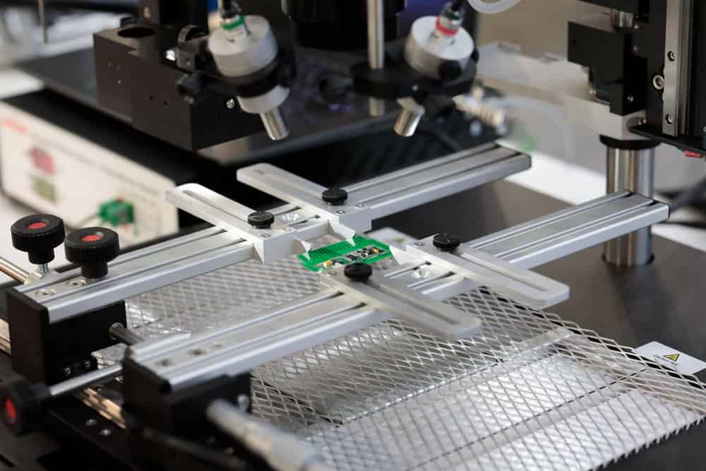
(Caption: Image of BGA soldering station)
Thanks to the reflow oven, BGA boasts an elaborate soldering to any PCB.
Remember, QFP pins’ close spacing requires careful soldering process control to align the package appropriately on the circuit board to prevent bridging.
For this reason, a controlled BGA soldering process and temperature are vital to prevent shorting solder balls and enhance the formation of good joints.
Benefits of BGA Technology
BGA has several advantages over ordinary SMD electronic components, including:
High Density
BGA allows high interconnection density circuits, solving the issue of producing small packages.
See the production of dual-in-line and pin grid array packages required many pins.
Thus, the pins were closely spaced.
However, this method complicated the soldering process as the closeness between pins increased the risk of accidental bridging between the pins.
With BGA, manufacturers can insert more interconnection pins on the connection package, resulting in a higher chip carrier performance.
Heat Conduction
PCB assembly and PCB package have a lower thermal resistance than SMD electronic components.
Due to this low resistance, the integrated circuit generates a free heat flow to the PCB, preventing overheating.
Low-Inductance Leads
Inductance is responsible for the undesirable distortion or disruption of signals in high-speed electronic circuits.
And lower electrical conductors have reduced unwanted inductance.
So the short distance between the BGA package and PCB connection gives superior electrical performance than pinned devices, thanks to their low inductance.
What Is BGA Packaging
A ball grid array (BGA) is a surface mount package without leads. And manufacturers leverage this SMT with an array of metal spheres (solder balls) for electrical connection.
This process involves attaching solder balls to a laminated substrate at the package’s bottom.
With this packaging, you connect the BGA’s die to the substrate using flip-chip technology and wire bonding.
Also, the BGA substrate has internal conductive elements that facilitate connection and routes the die-to-substrate to the rest of the substrate to bond arrays.
BGA Package Types
Developers have crafted various BGA variants to meet diverse requirements of various types of equipment and assembly.
These BGA package types include:
MAPBGA – Moulded Array Process Ball Grid Array
This package focuses on low to mid-performance gadgets that need low-intensity packaging to ease surface mounting.
This BGA offers a budget package option with a high-reliability level and a small footprint.
PBGA – Plastic Ball Grid Array
This PGA package is ideal for mid to high-performance devices that need low inductance, relatively low cost, ease of surface mounting, and high levels of reliability.
Also, the package type boasts additional copper layers within the substrate to enhance the ability to handle power dissipation.
TEPBGA – Thermally Enhanced Plastic Ball Grid Array
PGA packages in this category support higher levels of heat dissipation.
Thus, this package relies on thick copper planes in the substrate to relay heat from the die to the customer board.
TBGA – Tape Ball Grid Array
The package offers a solution for mid to high-performance level applications requiring high thermal performance without an external heatsink.
PoP – Package on Package
This package is ideal for applications featuring premium space. Also, it allows for stacking memory packages on your base device.
MicroBGA
As the name suggests, this BGA is smaller than a typical BGA package. Also, it comes in three prevalent pitches – 0.65mm, 0.75mm, and 0.8mm.
BGA Assembly
BGA assembly was among the core concerns during the inception BGAs.
One frequently asked question was whether BGA assembly could match the standards of a traditional SMT package.
And the fact that BGA packages are inaccessible was the leading cause of concern.
While soldering appeared to be the main problem for BGA devices, developers established that standard reflow methods worked for these devices, creating potent joint reliability.
And since then, BGA assembly approaches have advanced, making soldering even more reliable than ever.
Now the soldering process involves heating the overall assembly.
That’s because the solder balls have highly controlled amounts of solder which melts whenever it receives heat during the soldering process.
Additionally, the ample surface tension aids the molten solder in holding the circuit board and the package in desirable alignment as the solder cools and solidifies.
So the manufacturer chooses soldering temperature and alloy carefully to keep the solder in semi-liquid form and prevent it from melting.
BGA, Ball Grid Array Inspection
One shortcoming of BGA devices is that using optical methods to view soldered connections is impossible.
During the BGA pilot stages, manufacturers were unsure about the technology’s efficiency and ability to solder devices.
For one, it needs sufficient heat to ensure that all the balls within the grid melt efficiently to make effective joints.
Also, it’s challenging to test the joints exhaustively by checking their electrical performance.
That means there’s a heightened possibility of joints failing over time. So manufacturers rely on X-rays to inspect the device and examine the state of the soldered joint beneath.
However, the BGA devices solder work if you set the heat profile effectively to reduce resultant soldering problems. Thus, this property makes BGA assembly suitable for most applications.
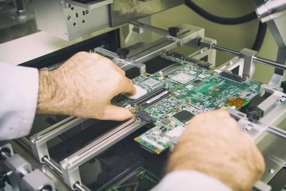
BGA Ball Grid Array Rework
Undoubtedly, it would help to have the correct equipment or tools to rework boards containing BGAs. Therefore, having the right tools helps remove a device if you suspect its BGA is faulty.
Remember, heat the solder underneath the device to remove the BGA package.
Interestingly, manufacturers achieve the heating during the BGA rework process by removing a specialized rework station.
And this process consists of a jig equipped with an infrared heater, a vacuum gadget to lift the package, and a thermocouple for monitoring temperature.
But you must exercise great care to ensure you only supply heat to the BGA to remove it.
Therefore, you must remove it with care to avoid damaging adjacent devices.
BGA Ball Grid Array Re-Balling
(Caption: Image of re-balling)
You can replace the BGA with a new one once you remove it. Sometimes, it’s possible to repair or refurbish the removed BGA.
The repair is necessary, especially if your BGA has an expensive chip that can still work after removing the device.
You can do a BGA repair using the ready-made solder balls the manufacturer produces and sells specifically for this purpose.
Interestingly, several companies have specialized equipment for BGA re-balling. And one of the most established technologies in this field is the ball grid array.
Technological innovations have enabled overcoming the challenge of inaccessible BGA contacts.
FAQs
Why Use a BGA in a Circuit?
BGA packages allow you to mount devices such as microprocessors permanently. The package provides more interconnection pins to align on a flat or dual in-line package.
What Is the Advantage of BGA?
BGA packages provide higher pin density, lower inductance, and reduced thermal resistance than typical packages. And these properties enhance interconnection pins and higher performance than flat or dual-in-line packages.
What Are the Disadvantages of BGA?
The pins beneath the BGA make it harder to inspect. In addition, because the pins are so delicate, one must exercise much caution when soldering. Otherwise, you risk damaging the pins and even displacing the BGA.
Further, the reflow soldering process heating makes the solder joint with the PCB pad vulnerable to flexural stress.
How Does a Ball Grid Array Work?
The ball grid array uses leads or solder balls to conduct electrical signals from the integrated circuit.
BGA uses solder balls placed within the PCB instead of pins like PGA.
Conclusion
BGA ball grid array is a game-changer in circuit technology that allows manufacturers to fit high-density pin connections.
Also, the immense benefits of BGA include increased efficiency and reduced package size.
These packages form the core of the products you desire to make, as they solve most of the problems that manufacturers face.
Therefore, comparing BGAs is essential in helping you make the best choice.