We all know what a PCB (Printed Circuit Board) is, its design, and its use cases. However, this might be your first time reading about a bare PCB board.
Like a PCB, a bare PCB board plays a critical role in the designing and developing of electronic products. Surprisingly, it’s a PCB without electrical components, making it possible to carry out cost-saving tests.
Consequently, you’ll have an efficient PCB fabrication and assembly process.
Please keep reading to understand bare PCB boards, their application, and testing.
Table of Contents
- What’s a Bare PCB Board?
- When to Use a Bare Board
- Bare Board Testing
- Bare Board Testing Types
- Benefits of Bare Boards
- Bare Board PCB Fabrication
- Errors in Bare Board Manufacturing
- FAQ
- Conclusion
What’s a Bare PCB Board?
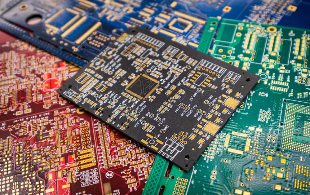
(Multi-colored PCB boards)
A bare PCB board has no electronic components or through holes. The board has a solder mask, metal coating, substrate, conductive pathway, and patterns.
Generally, the conductive pathways and patterns function to direct current to flow through the circuit.
Also, you’ll hear people referring to a bare PCB as etched wiring boards of PCBs. Surprisingly, bare PCB boards are developed with the single purpose of being populated with electronic components.
Therefore, they’re critical in manufacturing PCBAs (Printed Circuit Board Assemblies).
Moreover, bare boards don’t have electronic components, so they help conduct several tests.
When to Use a Bare Board
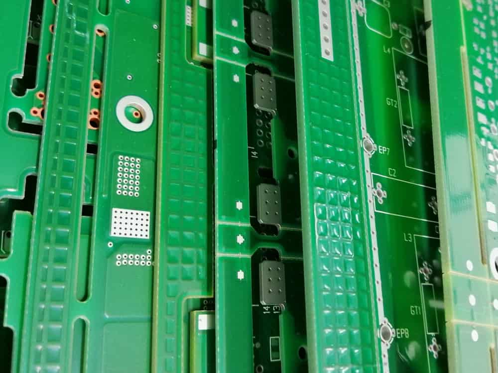
(bare board types)
A bare is designed to be configured, so you can use it to test its concept, functionality, and design before you assemble more expensive components. Therefore, it’ll offer mechanical support to pads, traces, and components.
Generally, a bare PCB board is a critical element required for PCB fabrication and design. Surprisingly, you’ll need it for almost every electronic production.
It’s in your best interest to use it for testing to preempt potential problems that might arise during or at the end of the fabrication process. Consequently, you’ll enjoy the usability of your electronic device.
Bare Board Testing
Bare board testing involves testing the isolation and continuity of a bare PCB board connection before adding components. An isolation test ensures that any two separate connections have the required resistance.
On the other hand, a continuity test ensures that the circuit has no open points. Consequently, current will flow freely through the circuit.
Bare board testing can save you much headache, including thousands of dollars you might be forced to spend for repairs and replacements. The test helps you identify issues early in manufacturing and make appropriate fixes.
Generally, bare PCB board testing streamlines the whole PCB fabrication and electronic design process.
Bare Board Testing Types
PCB companies will employ any of the below methods to do bare board testing:
Pinned Fixture Test
Here, spring-loaded pogo pins will test the bare board at once. They use the bottom and top plates to pressure the pin fixture to ensure connectivity across the bare board.
Generally, you can use this method to test thousands of points simultaneously. Surprisingly, it’ll only take five seconds to complete the testing.
Flying Probe Test
Here, you’ll use two robotic arms with poles to verify connections. Also, a software program feeds the flying probe with instructions as it moves across the connections.
This method will take longer to complete than the pinned fixture test. However, it offers flexibility and better affordability.
Automated Optical Inspection (AOI)
This method uses a 2D or 3D camera to photograph and compare your bare board with a schematic. You can flag the bare board for inspection if it fails to match the schematic. However, this method might require you to complement it with other methods.
Burn In Test
The burn In test allows you to test the bare board and, at the same time, establish its load capacity. It lets you run a power supply through the PCB at an elevated temperature.
You’ll have to do this for about 48 to 168 hours. However, the high temperature involved might destroy your bare board.
X-Ray Inspection
Here, you use x-rays to uncover defects you can not spot with the human eye. Surprisingly, it allows you to identify barrels, internal traces, and solder connections.
Benefits of Bare Boards
Apart from providing mechanical support to various PCB components, a bare board offers the following benefits:
Early Defect Detection
If you’ve ever tested PCBs, you understand they’re easier to test when they don’t have components. You can examine your board, assess any issues, and rectify them before completing the circuit.
Cost Saving
The board design and testing process ensures that the board is durable and functional. Therefore, you can detect any problems that might be difficult to fix later. Consequently, you won’t have to make erroneous assembly, especially for expensive components, thus saving money.
Time Saving
You’ll get satisfactory and design-specific functionality if you do good testing. Therefore, you won’t waste your time developing an ineffective PCB. Also, the testing process is automated and thus faster.
Bare Board PCB Fabrication

(PCB fabrication)
Check the bare board fabrication process below:
Drilling
Drilling allows you to create holes. Therefore, you must be careful during this process to avoid causing errors.
Hole Metallization
After drilling, you take the PCB through a conveyorized line. Consequently, holes are lined with carbon to form the cathode.
Photo Mech
Now, you use a photosensitive film plating resist to laminate the drilled bare board. Afterward, you use a direct imaging machine to image the board.
Plating
Here, the bare PCB board is copper-plated using periodically pulsed plating. However, be cautious to ensure the right copper amount is in the panels.
Etching
After that, you remove any unwanted copper from the bare PCB by dipping the board into an etching solution. Therefore, ensure you don’t expose the board to over or under-etching.
Solder Mask Application
You can then apply solder masks to the two sides of your bare PCB to protect the copper surface. Additionally, it prevents solder shorting of PCB components during assembly. Furthermore, it prevents trace disconnections.
Screen Printing
You press ink on the mesh screen to specify important information on your bare PCB. Additionally, screen printing helps to identify logos, marks, and parts on the board.
Finishing
You use electroless nickel immersion silver or gold for the exposed copper pads at this stage. Also, it would be best to use X-ray equipment to verify coating thickness.
Inspection
Finally, you inspect your bare PCB thoroughly.
Errors in Bare Board Manufacturing

(An old bare PCB)
The following problems may arise while manufacturing a bare PCB:
Extra Holes
You might drill too many holes in your bare PCB during the drilling phase. Generally, many holes cause errors during fabrication by reducing the available space.
Also, they reduce the routing area designed for signal tracing.
Excessive or Inadequate Copper
Copper is used in bare PCB as a conductive material for transmitting signals. However, having excessive or inadequate copper causes defects on the bare PCB. Surprisingly, excessive copper causes corrosion. Additionally, inadequate copper might cause short circuits.
Short Circuit Issues
As mentioned above, this might result from inadequate copper. Additionally, it results from wires getting into contact. Luckily, you can fix this issue by replacing the wires.
FAQ
How much does a bare PCB cost?
We approximate a bare board to cost between 5 cents to $300 to produce. However, the exact cost depends on the quantity, complexity, number of layers, and components involved.
Why is bare board testing necessary?
Testing allows you to identify any errors or problems during the early stages. Consequently, you can fix them, thus saving money and time in the long run.
What is the lifespan of a bare board?
All PCBs, including a bare PCB, can last 50 to 70 years. You need to keep it in the best condition to last longer.
How can you store your bare board?
Always store your bare PCB in a moisture-free environment. Therefore, we recommend a vacuum-sealed moisture-free bag.
Conclusion
A bare PCB board is necessary to design and develop electronic devices. Surprisingly, you can use it to test PCB concept, functionality, and design before you assemble more expensive components to build a fully functional PCB.
Consequently, you’ll benefit by saving costs and improving the product value. However, bare PCB board fabrication is challenging, and errors might arise. In the case of short circuits, replace the wires.