What are PCB boards? The world is undergoing changes, and at the center of it is technology. We have seen the development of electronic devices to manage almost every life aspect.
Surprisingly, many don’t know that these electronic devices come with a printed circuit board (PCB).
But what are PCB boards, where can you use them, and how are they designed? For answers to these questions and more, keep reading.
Table of Contents
- What Are PCB Boards
- Application of PCBs
- Types of PCB
- PCB Manufacturing Process
- Top PCB Design Programs
- FAQ
- Conclusion
What Are PCB Boards
PCB is an abbreviation for Printed Circuit board. Generally, it’s a board having printed wires that allow electrical connectivity. A PCB board might have a single layer or multiple circuitry layers.
Additionally, it has a low-conducting dielectric material with dielectric layers and metal to provide proper conductivity. PCBs, find applications in electronic components like smartphones, dishwashers, or televisions.
Application of PCBs
You’ll be surprised to learn that PCBs are in use everywhere, from automotive to medical devices. Below are specific areas you can find a PCB in use:
- PCBs, find application in medical devices like ultrasonic scanners, pacemakers, and CAT imaging systems. Additionally, they find application in blood glucose monitors and blood pressure monitors.
- PCBs are finding typical applications in automobiles, especially in manufacturing electric cars. They are specifically used in control, sensor, entertainment, and navigation systems.
- You’ll find PCBs in manufacturing equipment like the electric drill and temperature control devices.
- Light Emitting diodes which find common applications in computer displays, residential homes, and hospitals.
- In defense systems such as computers, control systems, firearms, and communication equipment. Additionally, PCBs find application in military aerospace, especially in flight systems.
- Nowadays, at least every consumer product has a PCB inside. The products include computers, home appliances, phones, earphones, and radios.
- PCBs, find common use in the oil industry for monitoring and downhole sensors.
Types of PCB
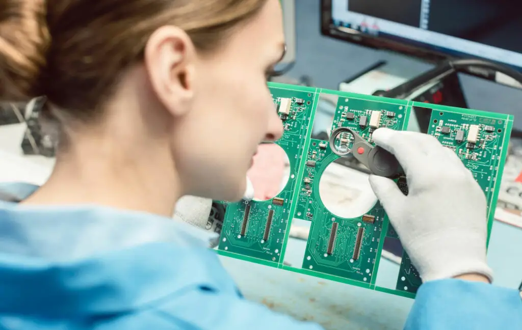
(A lady soldering components to PCB)
Now that you know where PCBs find application, let’s look at the different types of PCBs:
Single Layer PCB
A single-layer PCB comes with one layer of substrate or material. On one side, it’s laminated with a metal layer.
Here, copper is the most commonly used metal. These PCBs find common use in consumer electronics and d microwave capabilities, including radios, appliances, smartphones, and laptops.
Double Layer PCB
This PCB has a metal layer on either side of the substrate. Generally, they find applications in consumer electronics like smartphones and amplifiers.
Also, you can find them in interposer technology connecting two PCBs.
Multi-Layer PCB
This PCB has at least three copper conductive layers. You’ll find them in high-density interconnect (HDI) PCBs which find application in aerospace and medical fields. Additionally, they’re common in smartphones and other digital devices.
Flexible PCB
A flexible PCB comes with thin, flexible materials to fit into specific systems. In most cases, they find application in the same areas as a one-layer circuit.
Rigid-Flex PCB
The Rigid-Flex PCB is a multilayer PCB with both rigid and flexible materials. Generally, it’s a 3D interconnect that you can fold and bend into any shape. Surprisingly, they can have up to 50 layers.
High-Frequency PCB
These PCBs find application in high-technology HDI and are known for having low thermal expansion levels. You’ll find them in RF microwave technology and high-speed communications.
Aluminum Backed PCB
This PCB relates to thermal conductivity and heat removal from a PCB. Generally, aluminum helps to draw out from the PCB faster, thus enabling it to work effectively. You’ll find it in use in RF communications.
PCB Manufacturing Process
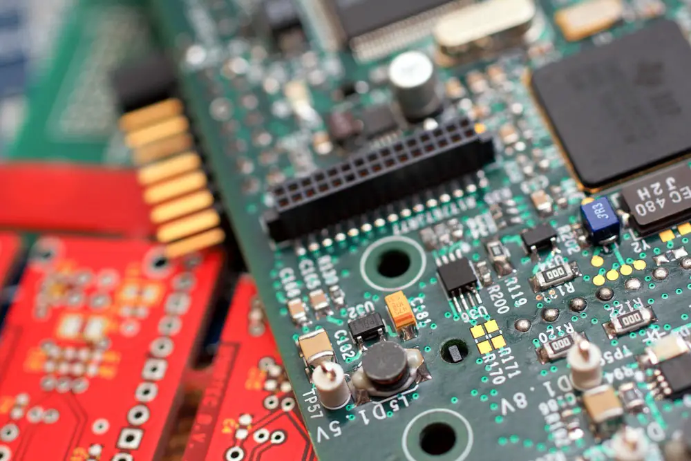
(A PCB photo)
The PCB manufacturing process is complex but manageable if you understand the steps. Check the steps below:
The Design
First, there is the development of a basic design. At this point, there is already a detailed circuit board blueprint.
The Print
Here, the PCB goes through printing, producing a resultant film that displays the different circuit board layers.
Generally, the clear ink will represent non-conductive areas, while black ink stands for the conductive copper pathways.
This applies to the inner layers. Therefore, the representation reverses for the outer layers.
The substrate
This connects all the elements and comprises glass fiber and epoxy resin. The substrate is first semi-cured in an oven before etching the board design onto it.
The Layers
Here, blueprints are important in creating laminate of the inner layers. Additionally, a resist is a photosensitive film covering the laminate.
The resist will cover the laminate to help in the PCB’s alignment.
The Bonding
After that, the panels move to the room, where they’re hit with UV light to harden the photoresist layer.
The Refining and Inspection
Here, an alkaline chemical solution helps to get rid of unwanted copper. After that, automated machines inspect the layers to ensure everything aligns in place.
Lamination, Pressing, and Drilling
We expect the layers to be pressed together and laminated using prepreg. There is a layer of copper foil and substrate over the prepreg.
Therefore, a mechanical press will press everything together and punch pins through to keep them in position.
After that, pressure and heat are applied to fuse the layers. Finally, the computer-guided grill drills into the different holes to expose the substrate and inner panels.
The Plating
Panels undergo cleaning and bathing with a series of chemicals—consequently, a thin copper layer deposits on the board’s surface.
Outer Layer Imaging
Again, a photoresist is applied while imaging the outer design layers. Afterward, UV light is used to harden it. At this point, we remove any unwanted photoresists.
The Plating
Here, you apply a thin copper layer to the board. Afterward, the board goes through tin plating to protect underlying copper pathways.
The Final Etch
At this point, you remove any unwanted and exposed pieces. Surprisingly, tin covers copper and prevents it from damage.
Consequently, there is a clear establishment of connections, pathways, and conducting areas.
Solder Mask Application
By now, the PCB is ready for solder mask application. However, before applying the solder mask, ensure the panels are clean.
Surface Finish
This finish is necessary to improve the element’s bonding to the PCB. Also, it increases the adhesion quality. Generally, you can use different materials, including gold and silver.
The Silkscreen
This involves using inkjet to print out important PCB information. Therefore, this is the last coat.
The Final Test
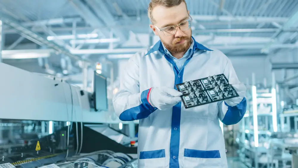
(An engineer doing a PCB inspection)
It’s important to run an electrical test on the PCB to ensure it’s working well.
In most cases, it’s done in an automated and controlled environment. Alternatively, a professional technician can do the test.
The Cutting
Lastly, after completing the testing, the PCB moves to a cutting machine which cuts the required number of boards.
You should have your final PCB, which you can use to design any electronic device.
Top PCB Design Programs
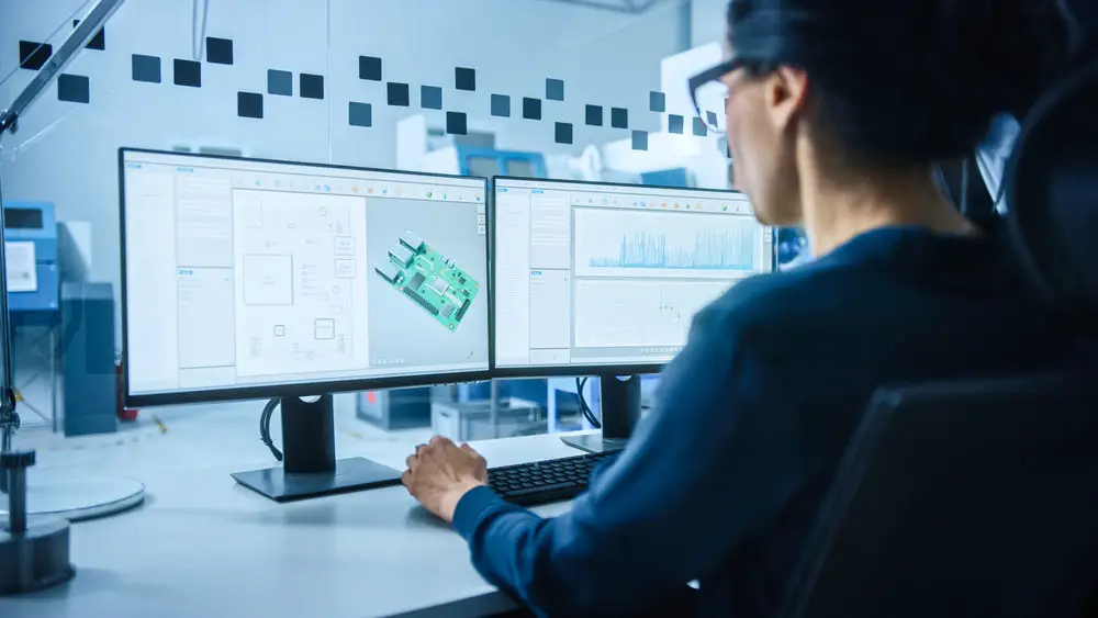
(An engineer using a design program)
What Are PCB Boards: Eagle
Eagle is a flexible editor that allows you to design PCBs and prototypes. The editor comes with a diagram editor diagram hierarchy to offer a better understanding.
Additionally, it provides for seamless annotation between your diagram and board. Furthermore, you’ll get layout diagrams having advanced features.
What Are PCB Boards: Altium
The program was initially called Protel Systems. Surprisingly, the programs layout routing design environment with diagrams and documentation.
Additionally, you’ll interact with 3D flex-rigid designs. Also, the program allows the output of production files.
Finally, there are several data conversion tools.
What Are PCB Boards: Proteus
This software offers the Proteus ISI and Proteus ARES. With Proteus ISI, you can create diagrams and electric simulations with ease.
On the other hand, Proteus ARES lets you manage PCB routing solutions with automatic component positioning.
FAQ
What materials are important for PCB layout design?
Generally, they use metals like iron, aluminum, and copper for PCB layout design. However, copper is the most common material in use.
What constitutes a good PCB layout?
Fundamentally, a good PCB layout should have its ground and power planes internally within the board.
Additionally, they should be at the center and regular to eliminate twisting and bowing of the PCB.
What is a PCB’s primary purpose?
A PCB offers mechanical support and electrical connection to circuit components. Nowadays, a PCB is available on almost every electronic device.
Conclusion
In conclusion, electronics are taking over the world and finding use in almost every aspect. Surprisingly, at the center of these devices are PCBs offering electrical connections.
For your PCB to work without problems, it should go through a reliable design. Well, we have highlighted the proper steps to follow above. Also, you can use Eagle, Altium, or Proteus for the PCB design.